| Apr 08, 2026 |
A review paper presents an integrated AFM framework for observing, manipulating, and engineering ferroelectric materials at the nanoscale for semiconductor applications.
(Nanowerk News) Researchers at KAIST have published a review paper that reframes atomic force microscopy (AFM) as an active platform for designing and controlling ferroelectric materials, not merely observing them. The review presents a unified analytical framework that integrates multiple AFM techniques to map electrical properties in three dimensions and directly manipulate material behavior at the nanoscale, with applications in next-generation semiconductor and energy device development.
|
Key Findings
- The review establishes an integrated AFM framework combining piezoresponse force microscopy, Kelvin probe force microscopy, and conductive AFM to construct three-dimensional maps of material structures and charge distributions.
- AFM has evolved from a passive imaging instrument into a research platform that can write, erase, and redesign ferroelectric domains through direct electrical and mechanical stimulation via its probe tip.
- The paper outlines future directions for pairing high-speed AFM with artificial intelligence to accelerate interpretation of complex nanoscale data.
|
|
Ferroelectric materials can hold an electrical polarization state without continuous external power, making them strong candidates for non-volatile memory and high-sensitivity sensors. As semiconductor components shrink deeper into the nanoscale regime, the physical phenomena at these dimensions increasingly determine overall device performance. Measuring and controlling electrical behavior at this scale with sufficient precision has remained a core technical obstacle.
|
|
The review, led by Professor Seungbum Hong from the Department of Materials Science and Engineering at KAIST, tackles that obstacle by laying out a systematic set of research strategies organized around AFM. Doctoral student Yeongyu Kim and integrated MS-PhD program student Kunwoo Park, both from the same department, served as co-first authors.
|
|
The paper was published as a front cover article in the Journal of Materials Chemistry C (“Atomic force microscopy for ferroelectric materials research”)
|
|
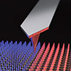
AFM works by scanning material surfaces with an extremely fine probe to capture information at atomic resolution. The instrument can function simultaneously as a sensor and as a tool for physical intervention, reading surface properties while also applying targeted electrical or mechanical inputs to alter them. This dual capability is central to the framework the review proposes.
|
|
The framework brings several specialized AFM modes into a single analytical system. Piezoresponse force microscopy (PFM) measures how a material deforms under an applied electric field, revealing the orientation and switching behavior of ferroelectric domains. Kelvin probe force microscopy (KPFM) maps variations in surface potential across a sample. Conductive AFM (C-AFM) tracks current flow through the material at specific locations. Combined, these methods yield a three-dimensional picture of internal structures and charge distributions that no single technique could provide alone.
|
|
What distinguishes this framework from conventional AFM use is the emphasis on active manipulation. By delivering electrical pulses or applying mechanical pressure through the probe tip, researchers can write and erase ferroelectric domains at precise nanoscale positions. This converts AFM from a characterization instrument into a prototyping tool, allowing device concepts to be tested at their intended operational scale before full fabrication.
|
|
The review also documents applications for evaluating emerging semiconductor materials. Two-dimensional transition metal dichalcogenides such as molybdenum disulfide (MoS₂) and ultrathin hafnium-zirconium oxide (HfZrO₂)-based films are both under active study for advanced memory and logic devices. The integrated AFM framework offers a route to assess and improve their ferroelectric performance at the single-domain level, providing feedback that bulk measurement techniques cannot deliver.
|
|
The research team also proposed combining high-speed AFM with artificial intelligence as a future direction. Nanoscale structures often generate dense, complex datasets that are difficult to interpret through manual analysis alone. AI-driven pattern recognition could accelerate the identification of structural features and domain behaviors, enabling faster screening of candidate materials and more targeted optimization of their properties.
|
|
“This study shows that atomic force microscopy has evolved beyond a simple observation tool into a key process technology for designing and precisely controlling advanced materials,” Professor Hong said. “Analytical techniques combined with artificial intelligence will play a critical role in securing technological competitiveness in next-generation semiconductor and energy materials.”
|
|
The framework outlined in this review positions AFM as infrastructure for ferroelectric materials development rather than a standalone measurement method. By combining nanoscale imaging, domain engineering, and multi-modal electrical characterization in a single instrument, the approach offers researchers a more direct connection between material properties and device-level performance, particularly as the industry moves toward thinner films and smaller feature sizes.
|