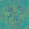
A nanophotonic diffractive network performs morphological image processing, including dilation and erosion, purely through light propagation.
(Nanowerk Spotlight) In the age of big data, we are generating more images than we can actually process. Autonomous vehicles, medical scanners, and quality control systems rely heavily on morphological transformations—the dilation and erosion of features in an image—to detect edges, remove noise, and identify defects.
Traditionally, these operations require capturing an image with a CMOS or CCD sensor, converting photons to electrons, and then performing thousands of logical operations in the digital domain. This electronic bottleneck not only introduces latency but also consumes significant power.
The device consists of spatially engineered diffractive layers. Once fabricated (or dynamically configured via a spatial light modulator), these layers act as a physical “program” that transforms the shape of incoming light patterns.
A free-space optical diffractive processor performs morphological transformations directly on incoming wavefronts. Unlike digital systems that require a sensor and extensive computation, this device modifies visual information as it propagates through passive diffractive layers. (Image: Yuxiang Sun and Jingtian Hu) (click on image to enlarge)
The core innovation lies in how the system handles structuring elements—the small matrices used in traditional image processing to probe shapes. In a digital computer, applying a structuring element to a large image is a sliding-window operation that requires thousands of multiply-accumulate operations.
In this new diffractive network, the structuring element is not a piece of software code; it is physically encoded into the surface relief and phase delays of the optical layers. Light carrying the image interacts with these layers once, and the desired eroded or dilated image appears at the output plane.
This shift from time domain to spatial domain computing results in dramatic performance gains. The authors experimentally validated their system using a reflection-mode setup with a total optical path measured in centimeters. The latency, therefore, was limited only by the speed of light traveling that distance—approximately 0.1 nanoseconds.
In numerical simulations for fully fabricated monolithic devices, the axial length can be reduced to just 380 micrometers (635 nm wavelength), suggesting theoretical processing times in the picosecond range.
Adaptive and Anisotropic Control
One of the major hurdles in analog optical computing has been the lack of flexibility—once a lens or mask is fabricated, its function is fixed. This team overcame this limitation by designing their diffractive networks through a deep-learning-based optimization process. This framework allows them to tune the “structuring element” digitally during the design phase, enabling the system to be highly anisotropic.
This is particularly relevant for applications like autonomous driving. A standard symmetric structuring element will dilate a road scene uniformly, which is often not desirable. The authors demonstrated direction-selective erosion that preserves thin horizontal lines (e.g., lane markings) while eroding vertical noise. This level of feature-specific extraction is achieved without any post-processing software.
Computing at the Sensor Edge
Another significant aspect of this work is its implication for edge computing. By modulating the wavefront before it ever hits a sensor, the platform acts as a pre-processor. This is especially valuable for phase information, which is lost the moment an image is digitized by an intensity-based sensor. Because the diffractive layers operate on the complex field (amplitude and phase), they can extract morphological features from transparent biological samples without first converting that phase data into pixel intensities.
Furthermore, the authors demonstrated that these modules are cascadable. By stacking diffractive networks, they performed compound operations such as opening (erosion followed by dilation) and closing (dilation followed by erosion), successfully denoising heavily corrupted images.
Conclusion
While digital computers continue to scale under the laws of Moore and Dennard, the fundamental energy cost of moving data from the sensor to the memory to the ALU remains stubbornly high. This research demonstrates a viable alternative: nanophotonics-based analog computing that processes information exactly where it exists—as light. By achieving morphological transformations with zero electronic logic, this platform offers a glimpse into a future where “processing” is as instantaneous as the propagation of light itself.
Source: By Jingtian Hu, Harbin Institute of Technology (Shenzhen), and Yuxiang Sun, The Chinese University of Hong Kong (Shenzhen)
For authors and communications departmentsclick to open
Lay summary
Prefilled posts
Nanowerk Newsletter
Get our Nanotechnology Spotlight updates to your inbox!
Thank you!
You have successfully joined our subscriber list.
Become a Spotlight guest author! Join our large and growing group of guest contributors. Have you just published a scientific paper or have other exciting developments to share with the nanotechnology community? Here is how to publish on nanowerk.com.