Plasma forms in gaps ten times smaller than classical theory predicts possible, driven by electron cascades on the substrate surface, enabling 2 W terahertz generation on a chip.
(Nanowerk Spotlight) Radio transmitters, microwave ovens, infrared cameras, visible lasers: every major band of the electromagnetic spectrum has its own well-developed technology. The exception lies between microwaves and infrared, a frequency range known as the terahertz band.
Terahertz waves oscillate between 0.1 and 10 trillion times per second. Modern airport body scanners already use them to reveal concealed objects through clothing without the health risks of X-rays. But terahertz waves can do much more: identify molecules by their vibrations, image biological tissue at high resolution, and carry wireless data at rates far beyond current standards. Making these applications portable and affordable requires a terahertz source that fits on a chip, the way a laser diode or radio transmitter does.
A device reported in Advanced Science (“High‐Power Terahertz Emission from Picosecond Nano‐Plasma Switching Driven by Secondary Electron Emission Avalanche”) takes an unexpected approach: instead of using semiconductor materials, it generates terahertz radiation by igniting plasma in an air gap narrower than a single virus particle. In this device, called a nano-plasma device, two metal electrodes sit 100 to 500 nm apart on a substrate, connected to a resonant circuit tuned to oscillate at a specific terahertz frequency.
A microwave pulse gradually charges the circuit while the nanogap remains insulating. When the electric field across the gap grows strong enough, air ionizes into plasma, a gas of free electrons and ions that conducts electricity. The gap snaps from insulator to conductor within about one picosecond, a trillionth of a second, and all the stored energy discharges into the resonant circuit in a single sharp pulse. The circuit then rings at its tuned frequency, producing 2 W of peak power at 0.4 THz, orders of magnitude above conventional chip-scale terahertz sources.
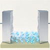
Overview of nano-plasma device for THz generation. (a) Schematic of picosecond nano-plasma switching driven by the SEEA, forming an ultra-dense electron sheet and nano-plasma. The input signal, output THz signal, and device components are illustrated. (b) SEM image of the system design, including the microwave input, output port, and the NPD composed of a waveguide structure, LC resonator, and nanogap (red-circled). (c) Breakdown voltage as a function of gap length. Three regimes, including the classic Paschen regime (>∼10 µm), the micro-discharge regime (∼1–10 µm), and the nano-plasma regime (<∼1 µm), are indicated. The tunneling limit at ∼1 nm and the Paschen minimum are also shown. (d) Measured down-converted THz signal generated by the nano-plasma device. A 0.4 THz signal with a peak power of 2 W was measured. (Image: Reproduced from DOI:10.1002/advs.75300, CC BY)
No established model predicts that plasma can form in a gap this small. Classical discharge theory sets a minimum of about 1.7 µm, determined by how far electrons must travel before colliding with gas molecules and triggering an ionization chain reaction. A 100 nm gap is more than ten times below that threshold. The devices work, but until now the physics behind them remained unexplained.
The answer lies not in the air but on the substrate surface. Field-emitted electrons from the cathode do not ionize air molecules during flight. Instead, they strike the substrate beneath the gap, and each impact knocks out multiple secondary electrons.
Those secondaries accelerate under the electric field, hit the surface again, and release more. This cascade, called secondary electron emission avalanche, sweeps across the substrate in about 0.1 ps and builds what the researchers call an ultra-dense electron sheet, a layer of electrons hovering within 10 nm of the surface at a density of about 10²⁵ per cubic meter.
The electron sheet does not itself constitute breakdown. It carries little current because the electrons are held near the surface by the positive charges their impacts left behind. Instead, the sheet acts as a reservoir of seed electrons. Once enough accumulate, their collisions with surrounding air molecules trigger a conventional ionization avalanche that fills the gap with plasma within about 1 ps.
The model makes specific, testable predictions about surface charge density, electron sheet thickness, and switching time. All three quantities matched between analytical theory, particle-in-cell simulations that tracked individual electrons through the full avalanche, and experimental measurements across a range of gap lengths. The consistency across such different methods provides strong evidence that SEEA is the mechanism driving nano-plasma breakdown.
One immediate payoff is a rule for choosing substrate materials. Whether SEEA can initiate depends on the secondary electron yield of the substrate, the number of electrons each impact releases. High-yield materials including SiO₂, sapphire, LiF, and MgF₂ all produced terahertz signals. Low-yield materials including SiC, GaN, and diamond did not. On low-yield substrates, impacts deposited negative charge that repelled subsequent electrons and prevented the cascade. Devices on SiC suffered irreversible bulk breakdown, destroying the device without producing terahertz output.
Gap length must also fall within a specific window. Gaps longer than about 1 µm switch too slowly to generate terahertz frequencies. Gaps shorter than about 20 nm prevent SEEA initiation because electrons cannot travel far enough along the substrate to sustain the cascade before reaching the anode.
Higher ambient pressure accelerates the process by increasing the rate at which electrons ionize air molecules. Encapsulating devices in pressurized cavities could extend the viable gap range to larger dimensions. The pulsed, high-voltage operation of nano-plasma devices also matches well with triboelectric nanogenerators, which could supply the driving voltage without external power, enabling self-powered chip-scale terahertz sources.
The same physics that enables terahertz generation also poses a warning for other nanoscale devices. Air channel transistors that rely on ballistic electron transport must prevent SEEA-driven breakdown. The study recommends avoiding electron-substrate collisions and selecting low-yield substrates for those applications. Under high vacuum, where air ionization cannot occur, the ultra-dense electron sheet might persist indefinitely, potentially enabling new types of vacuum nanoelectronic devices for ultrafast electron optics.
What began as a mystery, plasma forming where physics said it could not, now provides a complete engineering toolkit: the right substrate, the right gap, and the right pressure to build compact, watt-level terahertz sources on a chip.
Get our Nanotechnology Spotlight updates to your inbox!
Thank you!
You have successfully joined our subscriber list.
Become a Spotlight guest author! Join our large and growing group of guest contributors. Have you just published a scientific paper or have other exciting developments to share with the nanotechnology community? Here is how to publish on nanowerk.com.