A soft electronic device built to mimic a brain synapse repairs itself after being cut in half, recovering most of its electrical function and memory within a day.
(Nanowerk Spotlight) Artificial synapses are electronic devices that store and process signals in the same place, mimicking a basic feature of biological neural circuits in which connections strengthen or weaken with activity. They are attractive building blocks for neuromorphic computing and for bioelectronic systems that may someday interface with living nervous tissue. Making them work in soft, deformable form is a separate problem, and one with a stubborn weak spot: damage tolerance.
Each capability exists separately. Soft and stretchable synaptic transistors have been demonstrated, and so have self-healing electronics, mostly at the level of single conductors where bringing two cut surfaces back into contact restores a current path. Combining them at the transistor level is the unsolved part. A synaptic transistor stores its programmed state in a precisely ordered multilayer structure of electrodes, semiconductor channel, and gate dielectric, and a cut disrupts all three at once. Closing the polymer surface is not enough.
A study published in Advanced Functional Materials (“Self-Healing and Stretchable Synaptic Transistor”) describes a synaptic transistor that recovers at the full device level. After a blade severs it, roughly 80% of the operating current and over 90% of the memory function return within 24 hours, with no external trigger beyond mild warming. The transistor tolerates stretching, supports three-dimensional stacking and rolling, and produces electrical signals compatible with the nervous system of a live mouse.
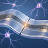
3S-T consists of a carbon nanotube composite as the SS-CNT conductor (top left), SS-pP bilayer layer as the insulator (top right), and SS-DPP-DTT as the channel (bottom right). The 3S-T array comprises 5 × 5 grid of source, drain, and gate lines, housing 25 3S-Ts (bottom left). Each unit 3S-T features MOSFET structure and maintains its memory state by dipole polarization (middle right). (Image: Adapted from DOI:10.1002/adfm.75662, CC BY) (click on image to enlarge)
The structure is built entirely from soft polymers. Carbon nanotubes embedded in a self-healing elastomer form the source, drain, and gate electrodes. The semiconductor channel uses an organic polymer called DPP-DTT mixed with the same elastomer. Above the channel, the gate insulator stacks two distinct materials: the elastomer below, with a softer fluorinated polymer from the polyvinylidene fluoride (PVDF) family on top.
The two insulator layers behave differently when stacked and heated than when processed apart. The fluorinated top layer can crystallize into several molecular arrangements, most of which produce only weak electrical polarization. Spin-coating it directly onto the elastomer below, then annealing the stack at 120 °C, encourages the molecule to adopt a zig-zag β-phase that produces strong, switchable polarization.
The phase shift is driven by attraction across the interface. A dipole is a small separation of positive and negative charge within a molecule or polymer chain. Slightly negative carbonyl groups in the lower elastomer pair with slightly positive hydrogen atoms in the fluorinated polymer above, supplying the energy needed to lock the chain into the β-phase. The bilayer behaves as a soft ferroelectric memory with a window about 3.8 times larger than the same materials annealed separately.
The two insulator polymers are chemically incompatible and refuse to mix. That immiscibility is what makes healing work. When a blade slices through the assembled device, each material aligns with its own kind across the cut rather than blending at the interface, and the cut surfaces re-form their original bonds at room temperature or under gentle warming. The semiconductor channel and electrodes follow the realignment of the surrounding polymer, and after 24 hours, the device’s transfer characteristics largely return.
Stretching tests revealed an instructive split between current transport and memory retention. Channel current declined steeply beyond 30% strain, but the memory window held its full size out to 50% strain in both pristine and healed devices. Charge transport through the semiconductor is sensitive to deformation; polarization stored in the gate dielectric is far more strain-tolerant.
The devices also displayed the gradual conductance changes used to model long-term potentiation and depression, the classical signatures of synaptic learning. Repeated voltage pulses pushed conductance up or down in small steps, allowing each device to represent a tunable synaptic weight. Pristine and healed samples behaved comparably, indicating that recovery preserved smooth analog modulation rather than only restoring on-off transistor switching.
To check whether the device’s output could communicate with a living nervous system, the researchers programmed the transistor to four conductance states and used it to drive electrical stimulation through a mouse’s forelimb nerves, recording the resulting brain activity in the somatosensory cortex. The amplitudes of the brain responses scaled with the device’s programmed weight, all within the 0 to 60 Hz range relevant to normal neural activity, placing the work alongside other efforts in adaptive implantable electronics that aim to match the mechanical and electrical character of soft tissue.
The same self-healing chemistry that repairs damage also bonds separate device modules together. The researchers stacked 5 by 5 transistor arrays into three-tier modules, rolled them into curved shapes, and connected the modules with a silver-flake composite as a stretchable interconnect. In one demonstration, two cells wired into a Pavlovian conditioning circuit responded more strongly to a previously neutral input after paired training pulses. The demonstration was not meant to reproduce animal learning, only to show that physically reconnected soft modules preserve circuit-level function.
A further test extended this principle to emulate structural neuroplasticity at the network level. Because the conductive interconnects can be cut and rejoined at will, connections between synaptic cells are themselves reconfigurable. Cells on the same tier, across stacked tiers, or in entirely separate modules can be wired together horizontally or vertically. A select-inhibit voltage scheme keeps each cell’s stored memory intact while operations target its neighbors, suppressing the crosstalk that usually plagues densely packed memory arrays.
The work remains an early laboratory demonstration. The transistors operate at relatively high gate voltages, raising power and safety questions for any future implanted use. The mouse experiment confirms electrical compatibility with neural tissue under acute conditions but does not establish chronic stability, immune response over months, or closed-loop therapeutic performance. The most consequential gap for this specific device concerns repeated damage-healing cycles: the paper characterizes a single recovery from a single cut, and a device intended for chronic use will need to survive many such events without cumulative drift in its programmed states.
The significance lies in treating self-healing as a full-device problem rather than as a property of a single material layer. The transistor does not merely use a repairable substrate or a stretchable conductor. It restores a multilayer structure whose programmed states can still be read after damage. For soft neuromorphic hardware destined to bridge electronics and tissue, the meaningful advance is not that the polymer heals, but that the memory survives.
For authors and communications departmentsclick to open
Lay summary
Prefilled posts
Nanowerk Newsletter
Get our Nanotechnology Spotlight updates to your inbox!
Thank you!
You have successfully joined our subscriber list.
Become a Spotlight guest author! Join our large and growing group of guest contributors. Have you just published a scientific paper or have other exciting developments to share with the nanotechnology community? Here is how to publish on nanowerk.com.