| May 18, 2026 |
A new approach controls low-cost solution processing of perovskites, improving the order of their thin layers for use in solar cells, LEDs and transistors.
(Nanowerk News) Perovskites are a class of materials with a unique crystal structure that suits applications such as fabricating solar cells, light-emitting diodes and transistors. However, the molecules in the thin layers often cannot arrange themselves properly because the process proceeds too quickly.
|
|
Now, an international research team led by Tomasz Marszalek from the Max Planck Institute for Polymer Research has developed a new approach to controlling low-cost solution processing, thereby improving the formation of well-ordered perovskite layers and enabling their broader application in optoelectronic devices.
|
|
They have published their results in the Journal of the American Chemical Society (“Crystalline Dion-Jacobson 2D Layered Sn-Based Perovskites for Field-Effect Transistors”).
|
 |
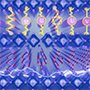
| Schematic diagram of a perovskite-based field-effect transistor. (Image: Katharina Maisenbacher / MPI-P)
|
|
Electronics can be found in almost every device, from smartphones and televisions to washing machines. Field-effect transistors are the main building blocks of electronic circuits — and ensure that these devices can be easily operated and fully controlled. Perovskites are a new class of semiconductor that could be suitable for transistor applications. They contain various chemical elements, such as organic cations, divalent metal cations, and halide anions. This combination of elements enables the properties of thin perovskite films to be tailored precisely for specific applications.
|
|
Currently, their use in transistors is often unsuccessful due to a lack of control over the formation of the thin film, known as “nucleation” and “crystallisation”. Therefore, researchers are attempting to organise the materials into thin, two-dimensional layers and stabilise them with organic molecules between the inorganic layers in order to control their optoelectronic properties.
|
|
The principle is similar to a double/single cheese burger, where layers of cheese represent the organic molecules that connect two layers of beef constituting the inorganic layers. Typical 2D perovskites are similar to a burger where the various layers are subsequently deposited, such that the double cheese is connected first to the underlaying beef.
|
|
However, in a special type of 2D perovskites, termed Dion-Jacobson, the single cheese has to be simultaneously connected to the under- and overlaying beef, making the construction of such a layered structure stronger but also far more difficult to achieve.
|
|
A research team led by Tomasz Marszalek of the Max Planck Institute for Polymer Research, in collaboration with colleagues from the Hong Kong Polytechnic University, the University of Toronto and the Norwegian University of Science and Technology, has developed a new approach that significantly simplifies the deposition of layered structures while improving the molecular organisation of two-dimensional Dion-Jacobson perovskite layers. These layers can then be used as semiconducting materials in transistors.
|
|
To achieve this, the team developed a method in which a solution of the starting materials slowly dries under solvent vapour (‘solvent vapour-assisted drop-casting’). This slow crystallisation process gives the building blocks more time to self-assemble into a uniform, well-ordered layered structure.
|
|
The team then systematically investigated a range of organic molecules (diammonium cations) that act as spacers and connectors between the inorganic layers and are responsible for the electrical properties. These unexplored molecules differed in stiffness and symmetry.
|
|
“Using thin film characterisation tools such as atomic force microscopy and X-ray diffraction, combined with theoretical calculations and electrical measurements, we were able to understand how these differences influence the crystal structure and conductivity — and thus hopefully lay an important foundation for applications of high-performance transistors,” says Tomasz Marszalek, a group leader in Paul Blom’s research group.
|
|
The researchers were able to demonstrate that particularly rigid and symmetrical molecules lead to greater order in two-dimensional Dion-Jacobson perovskites. These ordered structures facilitate the movement of electrical charge carriers through the material, which is a decisive advantage for future applications in electronic components.
|