| Apr 21, 2026 |
Researchers developed wet-etching-assisted single-pulse nanolithography to fabricate nanoholes in sapphire with depth-to-diameter ratios exceeding 50,000:1 for photonic applications.
(Nanowerk News) A research team led by Professor Jianrong Qiu of Zhejiang University and Professor Lijing Zhong of Ningbo University has fabricated nanoscale holes in crystalline sapphire with depth-to-diameter ratios exceeding 50,000:1. Their method, called wet-etching-assisted single-pulse nanolithography (WESPN), combines femtosecond laser nanolithography with deliberate optical aberrations and chemical etching, overcoming depth limits that have constrained sapphire nanofabrication and similar crystalline substrate processing.
|
Key Findings
- The method achieves nanoholes with sub-500 nm diameters and lengths up to 1,500 μm, yielding depth-to-diameter ratios greater than 50,000:1.
- Dense nanohole lattices function as waveguide cladding, guiding light through an unmodified sapphire core with high mode purity of 10.9 dB.
- Fluorescent probes embedded in the nanoholes confirm the waveguide’s optical sensing capability.
|
|
The work has been provisionally accepted in Light: Advanced Manufacturing (“Deep-nanohole-clad waveguides with depth-to-diameter ratio up to 50 000 in single crystals via femtosecond laser writing”).
|
|
Periodic arrays of subwavelength pores are the structural foundation of all-dielectric nanophotonic devices such as photonic crystals and metasurfaces. These structures enable precise manipulation of light and hold significant promise for optical communications, sensing, and quantum technologies. Their performance depends heavily on the constituent structural units maintaining extreme depth-to-diameter ratios, which has historically been difficult to achieve.
|
|
Conventional femtosecond laser processing struggles to produce high-aspect-ratio, densely packed nanostructures in glass and crystalline substrates. Two effects work against depth: nonlinear absorption saturates as the pulse propagates deeper into the material, and plasma defocusing disperses the laser energy before it can modify the target volume. Together, these effects impose a hard ceiling on nanochannel depth.
|
|
“We demonstrate a fabrication strategy that overcomes the long-standing depth limitation of single-pulse nanolithography by combining spherical-aberration-mediated focal stretching with dynamic axial stitching,” the scientists stated.
|
|
The WESPN approach works around these limits through a spherical-aberration-enhanced focusing strategy. The researchers directed a high-numerical-aperture objective to focus femtosecond laser pulses deep inside single-crystal sapphire. By deliberately introducing a refractive-index mismatch between the focusing optics and the substrate, the focal volume stretches along the optical axis rather than converging to a standard diffraction-limited spot. This elongated modification zone allows the laser to reach greater depths within the material.
|
|
To extend the nanoholes further, the team added dynamic axial focal stitching. The focal position is incrementally shifted along the depth direction, and successive single laser pulses create overlapping modification zones. After laser exposure, selective wet etching preferentially removes the laser-modified material, revealing continuous nanochannels with extreme aspect ratios.
|
|
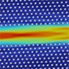
The resulting nanohole arrays serve a direct photonic function. When arranged in a dense periodic lattice, the air-filled nanoholes act as a low-refractive-index cladding surrounding an unmodified crystalline sapphire core. This geometry forms a nanophotonic waveguide that confines and channels light through the pristine crystal, achieving a mode purity of 10.9 dB.
|
|
The team further demonstrated that fluorescent probes inserted into the nanoholes can be excited by the guided light, confirming the structure’s viability as an integrated optical sensor.
|
|
“This unified approach offers a scalable route to functional photonic integration in hard crystalline substrates, opening new opportunities for quantum emitters, dense photonic circuits, and high-sensitivity biochemical sensing,” the researchers added.
|
|
Producing functional photonic structures directly inside hard crystalline materials, without compromising optical quality in the guiding region, fills a gap in current nanophotonic fabrication capabilities. The demonstrated waveguiding and sensing performance suggest that WESPN could serve as a practical route to integrated photonic devices in substrates that have traditionally resisted deep nanostructuring.
|