| May 08, 2026 |
Charge density waves in metals accumulate defects and melt much like physical solids, a behavior that could be harnessed for neuromorphic devices and superconductors.
(Nanowerk News) In a process analogous to how solids melt into liquids, the electrons in many different metals form crystal-like patterns that can deform and melt, opening new pathways for neuromorphic computing and superconductors, University of Michigan Engineering researchers have found.
|
|
“Our work shows that these quantum structures, which are often thought to have a highly ordered structure, actually span a continuum of disorder that could be leveraged to engineer and control these materials,” said Robert Hovden, associate professor of materials science and engineering and corresponding author of the study published in Matter (“Melting of charge density waves in low dimensions”).
|
|
“Metallurgists often control defects, or disorder, in metals to produce specific properties,” Hovden said. “A similar approach might help us harness the potential of quantum materials in future devices. Quantum metallurgy could be the future.”
|
|
The ability to precisely edit the structure of these electron crystals, also called charge density waves, could open new pathways for controlling superconductors—materials that transport electric current without resistance—since superconducting states can coincide with defects in charge density waves.
|
|
Controlling the structure of electron crystals could also allow engineers to rapidly turn metals into insulators, since charge density waves disrupt the flow of electricity in some conductors. Precisely switching between conductor and insulator mirrors the way brain cells transmit electrical signals, and some scientists think such materials could advance neuromorphic computing, which can process and transmit large amounts of data with little energy.
|
 |
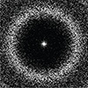
| The electron diffraction pattern of a fully melted electron crystal, based on predictions made by a computer model. (Image: Jeremy Shen, Hovden Lab, University of Michigan Engineering)
|
Electron crystals explained: Crystals within crystals
|
|
In a conductor, free electrons are typically distributed evenly throughout the metal. Sometimes, however, they form uniformly spaced clusters that create a wave-like pattern of alternating high and low electron density called a charge density wave.
|
|
This periodic clustering of charge resembles the atomic structure of crystals. When that order degrades, crystals physically melt, and it can happen in stages, especially when the crystal is only one or two atoms thick. Before the crystal melts completely, the distance between the atoms becomes more irregular and the rows of atoms dislocate. As a result, the sequential pattern breaks, creating tell-tale hexagonal motifs that repeat throughout the crystal lattice.
|
|
When scientists found the same intermediate melting state in charge density waves, some started to wonder if charge density waves could also melt completely. The structure wouldn’t flow like a physical liquid, but it would be a liquid in the sense that the ordered, periodic arrangement of electron clusters disappeared.
|
Melting the electron crystal
|
|
A white point on a black field is surrounded by many small points that create a halo-like pattern, also in white.The electron diffraction pattern of a fully melted electron crystal, based on predictions made by a computer model. Image credit: Jeremy Shen, Hovden Lab, University of Michigan Engineering.
|
|
Hovden’s team succeeded in melting a charge density wave inside a 2D sheet of the metal tantalum sulfide—although they couldn’t achieve a fully liquid charge density wave before the physical crystal started to change. As the electron clusters dislocated from their neat rows, the spacing between each row grew. The expanding structure increased the wavelength of the charge density wave pattern, which determines the conductivity of the material.
|
|
The researchers detected the melting by firing an electron beam at the metal as it was heated to 568 degrees Fahrenheit. When the fired electrons pass through the metal, they deflect off the atoms before hitting a camera. A spot is created at the impact site, and the arrangement of spots corresponds to the position and arrangement of atoms in the crystal.
|
|
When a metal has an electron crystal, the points that represent atoms in the diffraction pattern are surrounded by extra points that represent the positions of electron clusters. Hovden’s team found that these points smear into ovals and fade as the number of deformations in the electron crystal increases.
|
|
The researchers recreated the smearing pattern in a computer simulation that described how the melting electron crystal should diffract an electron beam. The simulation also described how the electron crystals could melt within an otherwise solid metal—the electron clusters disappear as the electronic pressure builds. Once a cluster vanishes, its composite electrons rejoin the background field.
|
|
The simulations also predicted that when the melting process completes, the diffraction ovals smeared into a faint halo surrounding the points that represent the metal’s atoms. This same halo pattern was found by researchers at UCLA after they created a liquid electron density wave.
|
|
Suspecting that the evidence for melting might have been hiding in older studies of charge density waves, Hovden’s team looked for the electron diffraction patterns in 28 studies of other metals with charge density waves. They found evidence of melting in nearly every 2D metal that they reviewed, as well as several 3D metals.
|
|
“When you look at these materials, they can have very different electrical and magnetic properties, but we can describe the core underlying physics of most of their charge density waves with this rather simple framework,” said Jeremy Shen, U-M master’s student in electrical and computer engineering and one of the study’s co-first authors. “The fact that we have one universal knob across all these systems that we could use to access different properties is very exciting.”
|
|
The charge density waves were studied at the Michigan Center for Materials Characterization, which is operated and maintained with support from indirect cost allocations in federal grants. The simulations were made with servers at U-M Advanced Research Computing.
|