| May 20, 2026 |
By aligning nanowires upright with an AC field before optical trapping, a hybrid method halves the laser power needed and boosts both trap success and speed.
(Nanowerk News) Optical tweezers use focused laser beams to trap and move tiny particles, but they struggle with high-aspect-ratio nanowires. The elongated shape of these structures creates strong scattering forces that often knock them out of the trap, while laser heating and surface adhesion further complicate precise manipulation.
|
|
Alternative methods using electric fields alone lack the fine spatial control needed for complex assembly tasks. Existing techniques also require high laser power, which risks damaging sensitive materials and living cells. Based on these challenges, there is a clear need for deeper research into hybrid strategies that combine multiple physical fields to achieve stable, gentle, and precise nanowire control.
|
|
Now, a team led by researchers at Beijing Institute of Technology, writing in Microsystems & Nanoengineering (“Nano calligraphy via optical electro-aligning manipulation”), reports an optical electro-aligning manipulation (OEM) strategy that integrates alternating current (AC) electric fields with holographic optical tweezers.
|
 |
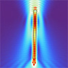
| a Simplified optical path diagram of the holographic optical tweezers. The optics include: a laser, a beam expander, 1/2 waveplates, a spatial light modulator, mirrors, lenses, a polarization beamsplitter prism, a condenser and a camera. A scanning electron microscope (SEM) image of the silver nanowires used in the experiment is shown on the screen. Scale bar: 1 µm. The dashed box indicates the location of the microfluidic chip, and the corresponding zoomed-in view of the chip and nanowire sample is shown on the right side of the image, where the electrical signal is generated by the signal generator and transmitted to the chip. b–d Schematic of the process of stably trapping nanowires using OT in an electric field. e–g Microscopic images of the electrically alignment process of nanowires: e Randomly oriented nanowires. f Upon powering on, nanowires orient and rotate. g In the steady state, the nanowires are vertically aligned. Scale bar: 10 µm (Image: Reproduced from DOI:10.1038/s41378-026-01225-0, CC BY)
|
|
The system first uses the electric field to rotate nanowires into a vertical orientation, then traps and moves them with dramatically improved stability and speed. The approach works on metal, semiconductor, and even biological nanowires.
|
|
The OEM method delivers three major performance gains. First, the trapping success rate jumped by 38% compared to conventional optical tweezers. Second, the laser power required for stable trapping dropped by half, from an average of 15 milliwatts to 7 milliwatts. Third, the maximum speed at which a trapped nanowire could be moved without escaping increased by 39%, from 26 to 36 micrometers per second.
|
|
These improvements come from a simple but powerful principle: applying the AC electric field first forces randomly oriented nanowires to stand vertically, aligning their long axis with the laser beam’s direction. In this orientation, the nanowire presents its smallest possible cross-section to the light, minimizing scattering forces while maximizing the gradient forces that hold it in place.
|
|
The team demonstrated the precision of their system by using a single nanowire as a pen to trace letters and intricate dragon shapes—a technique they call nano-calligraphy. They also showed parallel control of up to seven nanowires simultaneously and successfully applied the method to rod-shaped bacteria, confirming its compatibility with living samples.
|
|
“We basically give the nanowires a gentle nudge to stand up straight before grabbing them with light,” the authors said. “That small change makes a huge difference—it cuts the needed laser power in half and lets us move the nanowires much faster without losing control.” They explained that the electric alignment tames the random tumbling that normally makes nanowires so difficult to trap. “For the first time, we can write custom microscale patterns with nanowires as easily as drawing with a pen, and we can do it with multiple nanowires at once.”
|
|
This hybrid opto-electric platform enables lithography-free nanofabrication, allowing researchers to assemble complex patterns without expensive masks or cleanroom processes. Potential applications include bottom-up construction of nano-electro-mechanical systems (NEMS), quantum photonic circuits, and neuromorphic computing networks. The low laser power also makes the method gentle enough for biological work, such as positioning individual bacteria for single-cell analysis or building cellular nanoprobes.
|
|
By offering both precision and scalability, OEM bridges the gap between laboratory-scale nanowire experiments and real-world manufacturing, bringing functional nanodevices—from ultra-sensitive sensors to programmable bio-interfaces—closer to practical use.
|