| Jun 08, 2026 |
Van der Waals forces can tune ferroelectric thin films, improving control over material properties for smaller, more energy-efficient electronics.
(Nanowerk News) Researchers have demonstrated the ability to use van der Waals forces to tune the physical and electronic properties of ferroelectric thin-films. The work opens the door to new techniques for engineering materials for use in smaller, more energy efficient electronic devices.
|
|
“Epitaxy is when you deposit a crystalline layer of material on top of another crystalline layer of material,” says Yin Liu, co-corresponding author of a paper on the work (ACS Nano, “Heteroepitaxial Control of Thickness, Strain, and Domain Architecture in Few-Layer Ferroelectric Tin Monochalcogenides”) and an assistant professor of materials science and engineering at North Carolina State University. “When you are doing this with thin films, and the two layers are chemically bonded, the structure of those two layers have to match. However, if the two layers are bonded using van der Waals forces, the layers can have different orientations.”
|
|
“We wanted to see whether the relative strength or weakness of the van der Waals force influences the physical and electrical properties of an epitaxial material.”
|
 |
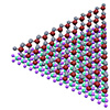
| Illustration of van der Waals heteroepitaxy, showing a thin film of ferroelectric tin selenide (SnSe) being deposited on a monolayer molybdenum disulfide (MoS₂) substrate. Researchers found that the strength of the van der Waals interaction between the two materials can tune the thickness, strain state and domain architecture of the resulting thin film, offering a new route for engineering low-power electronic materials. (Image: NCSU)
|
|
For this work, the researchers deposited a thin film of tin selenide (SnSe) on a monolayer of molybdenum disulfide (MoS₂). The researchers chose SnSe because it is widely studied in ferroelectric research; and MoS₂ because it is a material that can be easily integrated into electronic devices.
|
|
“We also chose these materials because MoS₂ has very close lattice matching with SnSe – meaning the crystalline structures are closely aligned,” says Liu. “This close matching means the van der Waals force is relatively strong. Previous work has looked at the properties of SnSe thin films deposited on other substrates, such as graphene, which had weaker van der Waals forces between the substrate and the SnSe. We wanted to see how the difference in van der Waals forces affected the epitaxial materials’ structure and properties.”
|
|
The researchers found that a combination of the lattice matching and strength of the van der Waals force affects three of the epitaxial material’s properties: its thickness, its strain state, and its domain architecture. Thickness refers to the number of crystalline layers in the material. The material’s strain state refers to how the material is stretched or compressed at the atomic level. And domain architecture refers to the polarization of discrete sections within the material.
|
|
“All of these characteristics have an effect on the material’s physical and electronic properties,” says Liu.
|
|
“Ultimately, this finding suggests we need to take a closer look at the role van der Waals force plays in influencing the properties of ferroelectric thin films, because it could be a valuable tool for engineering materials for a variety of applications.”
|
|
The researchers also found that using a monolayer of MoS₂ as a substrate allowed them to grow larger thin films of SnSe, in terms of lateral size or surface area, than has been demonstrated on previous substrates. And the thin films were higher quality, with fewer defects.
|
|
“This substrate is promising, and merits future investigation,” Liu says.
|