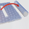
Electron-beam cuts make twisted graphene rebuild itself into carbon nanotubes, arrays, and Y-junctions through controlled edge chemistry.
(Nanowerk Spotlight) At the scale of atoms, a cut edge is not just a boundary. It is a line of unsettled chemistry, where atoms that once had stable neighbors do not simply wait in place but may now seek new bonds. In atomically thin carbon, that search can do more than repair damage. It can pull the material into an entirely different shape.
Carbon is well suited to this kind of shape change because the same bonding pattern can support several geometries. A single atomic sheet of carbon forms graphene. Two stacked sheets form bilayer graphene, and additional sheets create multilayer graphene on the way toward graphite. When a graphene sheet wraps into a cylinder, it forms a carbon nanotube.
Researchers can move among these forms in several ways, including unzipping carbon nanotubes into nanoribbons. The harder task is putting nanotubes where they are needed and joining them without losing control at nanometer dimensions. That challenge matters for nanoelectronics, quantum transport studies, interconnects, and channels that move molecules through confined spaces.
A paper published in Small (“Controlled Formation of Carbon Nanotubes and Nanotube Junctions from Bilayer Graphene”) by researchers at the University of Tübingen and Helmholtz-Zentrum Dresden-Rossendorf now shows how to use edge chemistry as a fabrication route. The team used a focused electron beam to cut narrow ribbons from twisted bilayer graphene, which consists of two graphene sheets rotated relative to each other. By cutting at half the bilayer’s twist angle, they made the exposed edges compatible enough to reconnect into nanotubes, arrays, and Y-shaped junctions.
a) Schematic representation of the carbon nanotube fabrication process, as two parallel lines are cut into twisted bilayer graphene to produce a nanoribbon whose edges then coalesce to form a chiral nanotube. The inset illustrates the relationship between the twist and cut angle required for the formation of a chiral nanotube. b) High-resolution transmission electron microscopy (HRTEM) image of a nanotube fabricated in this way. The inset shows the Fourier transform. The green lines indicate the relative twist angle between the graphene sheets. The red dashed line shows the cut angle and tube orientation in real space. Scale bar is 5 nm. (Image: Michael Schlegel, University of Tübingen) (click on image to enlarge)
The twist determines which cuts can reconnect cleanly. When two graphene layers sit at different rotational angles, most cuts expose edge patterns that do not match. A cut made at half the twist angle gives the two layers mirror-compatible edges, allowing carbon atoms to reconnect into a curved tube wall with fewer seam defects.
With the cutting direction set, the electron beam becomes more than a tool for removing carbon atoms. The team suspended chemical vapor deposition graphene over holes in heated support chips, identified clean twisted bilayer regions, and measured their rotation angles. They then used scanning transmission electron microscopy at 200 kV to mill the material along programmed paths.
The experiment depended on careful control of the environment around the cut. The sample stayed near 500 °C during cutting and imaging. Without heating, hydrocarbon contamination can attach to exposed bonds and defects, especially along fresh edges, and block the reconstruction needed for nanotube formation. The elevated temperature also made defect healing more likely, although the process did not produce flawless nanotubes.
The beam path gave the reconstruction its starting shape. Two parallel beam lines carved a narrow bilayer ribbon, while the spacing between them set the ribbon width. That width constrained the circumference of the tube that could form, rather than the diameter directly. When the ribbon was narrow enough, its open edges closed and the flattened bilayer unfolded into a tubular shape at a chosen location.
Not every ribbon could make that transition. Bending graphene into a tube costs elastic energy, while keeping two flat graphene layers in contact gains energy through van der Waals attraction. The experiments showed that ribbons below about 4 nm could form nanotubes, while wider structures around 4.5 nm remained flat. The authors placed the transition between collapsed and open tubular behavior near a tube diameter of 3.5 to 3.7 nm.
The researchers next tested whether the new structures were truly tubular, rather than flat ribbons with closed edges. They compared the edge contrast of each fabricated structure with that of nearby bilayer graphene in the same transmission electron microscopy (TEM) image. This local comparison helped account for imaging conditions that can shift contrast between images. Tube edges exhibited stronger contrast because the electron beam passes through more carbon atoms at a curved wall, confirming their cylindrical shape.
Atomistic simulations reproduced the same angle dependence. Molecular dynamics calculations began with twisted bilayer graphene ribbons and showed the open edges bonding together as each structure relaxed into a tube-like form. When the simulated cuts followed the half-twist rule, the tubes became rounder and contained fewer defects. Miscut ribbons formed rougher seams with more non-hexagonal carbon rings.
That control does not allow arbitrary nanotube geometries. Carbon nanotube properties depend on chirality, which describes how the graphene lattice wraps around the cylinder. The twist angle and cut direction can guide that wrapping, but they cannot produce any nanotube geometry on demand. Perfect nanotubes exist only for specific combinations of diameter and lattice angle. Random twist angles and arbitrary ribbon widths can approach a target geometry, but they cannot guarantee any chosen nanotube exactly.
The real tubes looked smoother than the simulated tubes in some comparisons. The authors suggest that time and temperature may explain the difference. In the experiment, structures remained at elevated temperature during extended observation, giving defects more opportunity to rearrange. The simulations compressed the transformation into tens of picoseconds at high temperature. Beam exposure could still add damage, so annealing and irradiation acted as competing influences.
The team showed architectural control by carving connected structures. Three ribbons cut at 120° angles formed Y-shaped nanotube junctions. Some branches stayed suspended, while others attached to nearby graphene edges. In one case, a branch broke and bent upward during electron-beam exposure, revealing a nearly circular cross-section and giving direct visual evidence for the tubular geometry.
The junctions add another level of control because they appear to connect hollow interiors. The images suggest that the two graphene layers remain separated through the junction, leaving an open space between branches. That feature points toward branched carbon channels for nanofluidics. Placing and connecting nanotubes also addresses a central challenge in nanoelectronics, where atomic structure can determine device behavior.
For now, the team’s approach suits precision experiments better than large-scale manufacturing. Focused electron-beam writing is slow, and the structures can move, deform, or attach to nearby material during fabrication. Seam defects, approximate chirality control, and beam sensitivity all limit device use. These constraints matter because many proposed nanotube devices depend on atomic structure as much as overall geometry.
The team showed that the beam does more than cut graphene. It exposes bonds that can make the remaining carbon rebuild itself. The beam writes boundaries, and those boundaries drive reconstruction. Here, the transformation comes from carbon bonds closing and relaxing into a new architecture.
For now, the technique remains a proof of principle, limited by speed, beam damage, and imperfect defect control. The result suggests that nanoscale cuts can do more than outline a shape. In twisted bilayer graphene, the right cut angle can guide how exposed edges close, how flat ribbons become tubes, and how separate tube interiors meet. Modified writing patterns, and possibly other layered materials, could extend this edge-driven approach to more complex, kirigami-like nanostructures.
For authors and communications departmentsclick to open
Lay summary
Prefilled posts
Nanowerk Newsletter
Get our Nanotechnology Spotlight updates to your inbox!
Thank you!
You have successfully joined our subscriber list.
Become a Spotlight guest author! Join our large and growing group of guest contributors. Have you just published a scientific paper or have other exciting developments to share with the nanotechnology community? Here is how to publish on nanowerk.com.