| Apr 09, 2026 |
Breakthrough findings offer new insight into spintronics to enable faster, smaller and more efficient devices.
(Nanowerk News) Data is growing at a staggering pace, pushing charge‑based microelectronics, such as smartphones and laptops, to their physical limits.
|
|
Spintronics — technology that uses electron spin rather than charge — avoids the limits of conventional electronics by switching information with very little energy, holding states without power and enabling extremely dense data storage.
|
|
Electrons possess a property called spin, which gives each one a tiny magnetic field that can point up or down, like a miniature compass needle. Because these magnetic orientations encode information, advancing spintronics requires controlling electron spins at the nanoscale.
|
|
Van der Waals magnets — ultrathin materials that can be peeled into layers only a few atoms thick — are ideal building blocks for spintronic devices, which rely on controlling electron spins and magnetic states at very small scales. Van der Waals magnets offer a powerful new platform for next‑generation electronics and data storage technologies.
|
|
In groundbreaking new research, scientists at the U.S. Department of Energy’s (DOE) Argonne National Laboratory reveal how magnetic domains behave inside these 2D van der Waals magnets. This finding provides a roadmap for designing and tuning future spin‑based technologies.
|
|
“AI’s growth is pushing the limits of today’s microelectronics. Spintronics could enable faster, smaller, more efficient devices to meet the demand,” said Amanda Petford-Long, materials science researcher emeritus, an Argonne Distinguished Fellow and a co-author of the study published in Advanced Functional Materials (“Thickness-Dependent Skyrmion Evolution in Fe3GeTe2 During Magnetization Reversal”).
|
 |
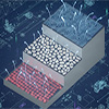
| A graphical representation of the 2D magnet Fe₃GeTe₂ with stepped thickness regions. Under a reversed applied magnetic field (indicated by arrows), distinct magnetic domain patterns emerge as a function of thickness, including stripe domains, patch-like domains and skyrmions. (Image: Argonne National Laboratory)
|
|
A key part of the study involved examining the underlying structure of magnetic materials at the domain level.
|
|
“Magnetic domains are regions where a material’s magnetization points in one direction or another — like tiny north–south poles. The team examined how these regions align and how they change under different external conditions,” said Charudatta Phatak, interim director and group leader in Argonne’s Materials Science division and a study co-author.
|
|
Specifically, scientists sought to understand how changing the thickness of a nanoscale magnetic material affects its domains. This includes how those domains form and switch and how thickness influences their density and size.
|
|
“The goal is to identify the parameters that control the spins in the material — specifically sample thickness and applied magnetic field,” said Jennifer Garland, a Northwestern University visiting graduate student at Argonne and a lead author of the study.
|
|
“Thickness strongly influences magnetic behavior. That means mapping these changes is essential for predicting and engineering the material’s properties,” said Phatak.
|
Direct imaging of magnetic patterns at the nanoscale
|
|
Researchers studied Fe3GeTe2 (FGT), a van der Waals ferromagnet known for its strong magnetic properties and potential for spintronic applications. Because FGT is only magnetic at very low temperatures, researchers cooled the sample with liquid nitrogen to about minus 173 degrees Celsius (around 100 Kelvin).
|
|
Scientists applied a magnetic field during this cooling process, known as field cooling. This allowed scientists to produce well‑defined magnetic patterns and generate different domain states on demand.
|
|
Each domain pattern exposed new details about how spins organize at the nanoscale. Previously, scientists had to infer a material’s domain structure from its overall magnetization. To probe these behaviors in even greater detail, scientists turned to direct imaging of how magnetic patterns evolve inside ultrathin materials using cryogenic Lorentz Transmission Electron Microscopy (cryo‑LTEM) at the Center for Nanoscale Materials (CNM), a DOE Office of Science user facility at Argonne. Cryo-LTEM is a technique that images magnetic structures in materials while they are cooled to cryogenic temperatures.
|
|
Researchers imaged a single flake of FGT and tracked its magnetic structures in real time during magnetization reversal.
|
|
Scientists discovered how material thickness and applied magnetic fields govern skyrmion size, density and evolution in the FGT magnet. Skyrmions are tiny magnetic whirlpools formed by twisting electron spins. They are incredibly small, remarkably stable and require very little energy to move.
|
|
“The overarching goal is to learn how to precisely control skyrmions so they can potentially be used in advanced, high‑density information technologies,” said Garland.
|
|
This finding is essential for shrinking skyrmions so they can match the tiny dimensions of today’s electronic components.
|
|
Micromagnetic simulations from collaborators at the University of Edinburgh (U.K.) reproduced the flake’s magnetic behavior and closely matched the cryo‑LTEM experimental results. The simulations were performed and analyzed using Argonne’s high performance computing resources.
|
Argonne unlocks new pathways for spintronics
|
|
Essentially, Argonne’s work offers a roadmap that allows scientists to predict the resulting domain patterns and their behavior for any given thickness and cooling conditions.
|
|
Mastering magnetism in atomically thin materials brings spin‑based, energy‑efficient computing closer to reality.
|
|
“If engineers can reliably tune skyrmion size and density, they can begin building the kinds of spintronic technologies that have long been imagined. Those with ultra‑dense memory, low‑power processors and magnetic storage far beyond the capabilities of today’s hard drives,” said Phatak.
|