A nanowire diode with a built-in electron trap senses, denoises, and classifies images without separate processing hardware, mimicking the retina and opening a path to smarter edge computing.
(Nanowerk Spotlight) The human retina does not simply photograph the world and forward raw data. Its cells detect light, suppress noise, and begin extracting patterns before any signal reaches the brain. Electronic image sensors work nothing like this. A modern smartphone camera contains millions of photodiodes, each surrounded by transistors that store and shuttle data to a separate processor.
The sensor captures an image, converts it to digital bits, ships those bits across the chip, and only then can software begin cleaning up noise or recognizing a face. Every transfer costs time and energy. Collapsing those separate stages into the sensor itself would require a pixel that can detect light, remember what it saw, and begin computing with that information, all without adding extra components.
Researchers have tried various workarounds, from neuromorphic transistors that integrate sensing, memory, and learning to swapping in unconventional materials such as two-dimensional semiconductors, perovskites, or ferroelectric films, but each approach adds fabrication complexity. A cleaner solution would be to leave the basic two-terminal diode structure intact and instead engineer its internal layers so that the junction itself can trap, store, and release electrons on command. In effect, a single diode could then serve as sensor, memory, and processor at once, a three-in-one neuromorphic chip that handles image capture, denoising, and classification without any supporting circuitry.
Because AlGaN has a wider bandgap, meaning electrons need more energy to move through it, this layer acts like a basin that photogenerated electrons can fall into but cannot easily escape. Electrons accumulate in this embedded reservoir, stay confined there, and can later be pulled out, all controlled solely by the voltage across the device’s two terminals.
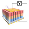
Figure 1. Performance of the integrated sensing-memory-processing diode. (a) Schematic diagram of the integrated sensing-memory-processing diode and its array. (b) Schematic bandgap structure of the device under three bias-tunable functions, where the inserted charge storage layer can store or release charges via the applied bias. (c) Self-powered square-wave photoresponse characteristics of the device under different light intensities at zero bias. (d) Photosynaptic characteristics of the device under different light pulses at a constant bias. (e) Photomemory characteristics of the device during optical write–voltage pulse read–voltage pulse erase cycles. (f) Schematic of the neuromorphic image sensor based on the integrated sensing-memory-processing diode. (Image courtesy of the researchers) (click on image to enlarge)
What the device does with those confined electrons depends entirely on the applied voltage. At zero bias, it works as a self-powered photodetector. Ultraviolet light at 265 nm knocks electrons free, and the junction’s built-in electric field sweeps them into a current that scales linearly with light intensity, yielding a responsivity of 10.45 mA W⁻¹. Some electrons settle into the AlGaN reservoir during illumination, but without an external voltage nudging them out, they remain confined and leave the sensing signal undisturbed.
Apply 1 V of forward bias and the device shifts into a second role: an artificial synapse. The voltage lowers the walls of the reservoir so that confined electrons begin leaking out, generating a persistent current that lingers after the light is switched off. Much as a biological synapse retains a chemical trace of recent stimulation, the diode “remembers” that it was illuminated. If a second light pulse arrives before the reservoir has fully emptied, the photocurrent builds on the residual level rather than restarting from zero.
This behavior replicates paired-pulse facilitation, a hallmark of synaptic plasticity, with a facilitation ratio reaching 122%. The output also grows with pulse number and frequency: strong, rapid stimulation produces large responses, while weak, sporadic signals yield small ones. That built-in frequency filtering, similar in spirit to the approach used in nanomaterial-based artificial synapses for neuromorphic image sensors, naturally separates persistent image data from random noise, enabling the diode to denoise an image without any external circuit.
The third mode, photomemory, emerges when light and voltage are applied at different times. At zero bias the diode captures photogenerated electrons in its reservoir, where they remain even after illumination stops. A subsequent voltage pulse extracts the confined charge as a readout current proportional to the accumulated light dose. A strong reverse bias then flushes the reservoir clean, completing a write–read–erase cycle. Because the readout current increases linearly with exposure, the device can encode eight clearly distinguishable current states, enough to store synaptic weights for a hardware neural network.
Fig. 2. Demonstration of neuromorphic imaging based on the integrated sensing-memory-processing diode array. (a) Image processing workflow and optical images of the imaging array and readout PCB, (b) Schematic illustration of real-time noisy image sensing, noise suppression, and image classification. (Image courtesy of the researchers) (click on image to enlarge)
The nanowires themselves are roughly 250 nm long and 30 nm in diameter, grown on a silicon substrate by molecular beam epitaxy, a technique that deposits material one atomic layer at a time under ultrahigh vacuum. The critical question was whether the three intended segments actually formed with sharp boundaries. Elemental mapping confirmed distinct regions of p-GaN (~100 nm), n-AlGaN (~100 nm, ~40% aluminum), and n-GaN (~50 nm), while clean lattice fringes and the absence of stray photoluminescence peaks confirmed high crystal quality, a benefit of strain relaxation in the slender nanowire geometry.
To test whether the concept holds up at scale, the team fabricated a 10 × 10 crossbar array on a readout printed circuit board. Performance across all 100 devices varied by less than ±5%, and endurance tests showed under 5% current drift over 50 write–read–erase cycles. With this array they ran a complete image-processing pipeline. Fashion-MNIST images were projected onto the array at zero bias alongside random noise, simulating real-world sensing. The bias was then switched to 1 V without re-exposing the array to light.
Pixels carrying real image data had deposited charge in their reservoirs; noise pixels had not. The readout voltage therefore amplified the true signal and suppressed the noise. The photomemory mode then programmed synaptic weights for a three-layer neural network that classified the denoised images. After ten training epochs, recognition accuracy exceeded 95%, compared with less than 60% for the raw noisy input, a gain of roughly 35 percentage points.
The gallium nitride nanowires used in this work respond primarily to ultraviolet light, which limits the range of practical imaging applications. However, the underlying principle, embedding a wider-bandgap layer inside a p–n junction to create an electron reservoir, is not specific to any one material. Adapting the approach to other semiconductor systems could extend the spectral response into the visible and infrared, opening the door to broader use.
Because the fabrication is compatible with standard CMOS processes and the device stays a simple two-terminal structure, it avoids the complexity that has held back three-terminal or exotic-material alternatives. Like earlier efforts to build silicon image sensors that integrate computation, this work points toward compact, energy-efficient edge-computing sensors, but goes further by collapsing sensing, denoising, and classification into a single diode array operating entirely in the analog domain, without ever converting signals to digital form.
For authors and communications departmentsclick to open
Lay summary
Prefilled posts
Nanowerk Newsletter
Get our Nanotechnology Spotlight updates to your inbox!
Thank you!
You have successfully joined our subscriber list.
Become a Spotlight guest author! Join our large and growing group of guest contributors. Have you just published a scientific paper or have other exciting developments to share with the nanotechnology community? Here is how to publish on nanowerk.com.