Nanoscale molybdenum disulfide memristors integrated onto standard CMOS chips achieve the lowest switching voltage reported for any 2D-material memristor on chip.
(Nanowerk Spotlight) Every time a conventional computer retrieves data from memory, electrical signals travel back and forth between the processor and a separate storage unit. That round trip costs energy and time, and it creates a fundamental bottleneck that chip designers call the memory wall.
One proposed solution is to store and process information in the same physical location using a device called a memristor, a resistor whose electrical resistance can be flipped between a high state and a low state by a voltage pulse and held there without power. Because this toggle resembles the way biological synapses strengthen or weaken, memristors are a key building block for neuromorphic computing, a field that aims to design circuits modeled on the brain rather than on traditional logic gates.
Two-dimensional materials have emerged as strong candidates for memristor construction. Molybdenum disulfide (MoS₂) is especially attractive: laboratory devices built from it have switched states at voltages below 0.3 volts, consumed less than 10 femtojoules of energy per operation, and survived more than a million switching cycles.
Yet nearly all such demonstrations have used isolated, micrometer-scale structures on simple silicon dioxide wafers, not on the dense multilayer wiring of actual silicon chips. Hexagonal boron nitride (h-BN), the only other two-dimensional material previously integrated onto CMOS platforms, requires five to ten times more voltage to operate, limiting its appeal for low-power applications.
A study now published in Advanced Functional Materials (“Integration of Low-Voltage Nanoscale MoS2 Memristors on CMOS Microchips”) addresses that limitation directly. A team based primarily at RWTH Aachen University and the Forschungszentrum Jülich in Germany has integrated nanoscale MoS₂ memristors into the back-end metal wiring of 350-nanometer-technology CMOS microchips, pairing each memristor with an on-chip transistor and demonstrating stable, low-voltage memory switching across 19 separate devices.
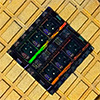
Au/Ag/MoS2/Pd memristor integrated on a silicon CMOS microchip. a) Optical photograph of a 350 nm node silicon CMOS microchip with integrated MoS2 memristors. b) Schematic of the MoS2-based one-transistor-one-resistor (1T1R) cell. The memristor is integrated on the fourth metal layer (M4), where Pt/Ta pads connect the third metallization layer of the BEOL interconnections to an n-channel CMOS transistor in the FEOL. c) Top-view scanning electron microscopy (SEM) image of a completed Au/Ag/MoS2/Pd memristor connected to the prepatterned Pt/Ta pads over the W vias. The inset shows a magnified view of the crossing of the top and bottom electrodes, defining an active area of ∼0.015 µm2. Inset scale bar: 500 nm. d) Cross-sectional high-angle annular dark field (HAADF) scanning transmission electron microscopy (STEM) image of a pristine MoS2-based 1T1R integrated cell. e-i) Energy-dispersive X-ray spectroscopy (EDXS) elemental maps confirming the presence of Au, Ag, molybdenum (Mo), sulfur (S), and Pd within the memristor. Scale bars in (e-i): 100 nm. (Image: Reproduced from DOI:10.1002/adfm.202527644, CC BY) (click on image to enlarge)
The researchers started with CMOS wafers containing n-channel transistors with metal interconnects routed up to a third metallization level. Instead of sealing the chips with a conventional passivation layer, they left the tungsten contact points exposed and deposited platinum and tantalum pads over them to form a fourth metal layer. This layer served as the electrical bridge between the memristors fabricated above and the transistor circuitry below.
The MoS₂ films, roughly 2.3 nanometers thick, were grown on sapphire substrates by metal-organic chemical vapor deposition and then transferred onto the prepared chips. Electron beam lithography defined bottom and top electrodes on either side of the MoS₂. The overlap between each electrode pair set the active device area at approximately 0.015 µm², the smallest cell size reported for any two-dimensional-material memristor, whether standalone or on a chip.
Each memristor was coupled with its adjacent CMOS transistor in a one-transistor-one-resistor, or 1T1R, configuration. The transistor acts as a precise current limiter during programming, suppressing parasitic effects and tightening the distribution of switching voltages. A standalone memristor tested on the same chip without transistor control showed noticeably greater variability, confirming the practical benefit of full CMOS integration.
The 1T1R cells switched without requiring an initial high-voltage “forming” step, a common prerequisite in many memristor technologies that adds complexity to circuit design. In 600 consecutive switching cycles on a single device, the set and reset voltages clustered tightly around their mean values, with cycle-to-cycle variability of the set voltage below 10 percent.
A separate endurance test on another device exceeded 4,000 switching cycles with no significant degradation of either resistance state. Retention measurements confirmed that both states held steady for at least 2.3 hours before the test was deliberately stopped.
All 19 tested 1T1R cells, each subjected to 100 consecutive switching curves, exhibited stable, forming-free operation with reliable distinction between resistance states. The lowest observed set voltage across the device cohort was approximately 0.23 volts, the lowest value reported for any two-dimensional-material memristor monolithically integrated on a CMOS chip. The corresponding reset voltage was roughly −0.1 volts. Cycle-to-cycle variability across the best-performing device was just 6.7 percent.
By adjusting the transistor gate voltage during programming, the researchers also demonstrated multilevel switching, encoding multiple distinct resistance levels in a single cell. This capability is essential for analog synaptic weighting in neuromorphic circuits, where graded signals rather than simple on/off states carry information.
To identify the physical mechanism behind the switching, the team examined devices using scanning transmission electron microscopy and elemental mapping. In a device held in its low-resistance state, silver from the top electrode had migrated through the MoS₂ layer and accumulated at the bottom electrode interface, forming thin conductive pathways bridging the two contacts.
An unswitched device showed no such silver between the electrodes. This migration pattern is characteristic of electrochemical metallization, a mechanism in which an applied electric field drives metal ions through a thin switching layer to build and dissolve nanoscale conductive filaments.
The combination of a nanoscale footprint, ultra-low operating voltages, forming-free behavior, and compatibility with standard back-end processing addresses several barriers that have kept two-dimensional-material memristors confined to isolated laboratory prototypes.
Scaling the process to full wafer dimensions, designing array-level read and write circuitry, and managing the inherent randomness of filamentary switching remain open engineering problems. But dense three-dimensional memory stacks, in-memory computing architectures, and artificial synaptic networks all depend on memory elements that can be manufactured reliably alongside conventional transistors.
With the smallest reported cell size and the lowest on-chip switching voltage for its material class, MoS₂ now has a working foothold on the platform where it will ultimately need to perform.
For authors and communications departmentsclick to open
Lay summary
Prefilled posts
Nanowerk Newsletter
Get our Nanotechnology Spotlight updates to your inbox!
Thank you!
You have successfully joined our subscriber list.
Become a Spotlight guest author! Join our large and growing group of guest contributors. Have you just published a scientific paper or have other exciting developments to share with the nanotechnology community? Here is how to publish on nanowerk.com.