A heat-resistant titanium dioxide scaffold makes it possible to nanoimprint reconfigurable phase-change metasurfaces over large areas, achieving infrared modulation and switchable chirality.
(Nanowerk Spotlight) A smartphone camera lens is several millimeters thick because conventional optics rely on curved glass to bend light. A metasurface can do the same job in a layer thinner than a human hair, using nanoscale patterns etched into a flat film. These ultra-thin optical surfaces have already proven they can focus, filter, and steer light with remarkable control.
Their potential expands dramatically when paired with phase-change materials. Chalcogenide compounds such as Ge₂Sb₂Te₅ can shift between amorphous and crystalline phases when heated, producing abrupt changes in refractive index. A metasurface built with such a material can switch its optical behavior on command, transitioning between distinct functional states without any moving parts. Such reconfigurable metasurfaces based on phase-change materials have attracted intense research interest for exactly this reason.
This tunability has already enabled prototype devices for non-mechanical beam steering, reconfigurable metalenses, amplitude modulation, and neuromorphic photonic computing. Yet nearly all of these demonstrations rely on electron beam lithography, a fabrication method that delivers superb resolution but operates slowly, over tiny areas, and at high cost. Free-space photonic applications, devices that manipulate light traveling through open air rather than through optical fibers or waveguides, demand centimeter-scale patterned surfaces, and electron beam writing simply cannot deliver them economically.
Nanoimprint lithography offers one alternative, stamping nanoscale patterns into a resist layer with high throughput and low cost. Researchers have already explored scalable printing methods for manufacturing metaoptics using nanocomposite materials, but conventional polymer-based resists melt or degrade at the temperatures required to crystallize and re-amorphize phase-change materials, which can exceed 600 °C. This thermal mismatch has left nanoimprint lithography unexplored as a route to reconfigurable phase-change metasurfaces, despite its otherwise excellent scalability.
The research team replaced the fragile polymer resist with a paste composed of 20 nm diameter anatase titanium dioxide nanoparticles. After imprinting, the patterned film is baked at 500 °C to burn away its organic binder, leaving behind a mesoporous TiO₂ scaffold capable of withstanding temperatures of at least 1000 °C. This thermally robust backbone is then coated with a thin film of antimony selenide (Sb₂Se₃), a chalcogenide phase-change material chosen for its low optical losses in both amorphous and crystalline states across the near- to mid-infrared.
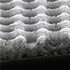
Schematics, optical properties, and morphology of large-scale nanoimprinted phase-change metasurfaces (a) Optical images of m-TiO2 imprinted arrays before (top) and after (bottom) deposition of Sb2. (Image: Reproduced from DOI:10.1002/advs.202521515, CC BY) (click on image to enlarge)
A central question for any nanoimprint approach is whether a simple stamping sequence can produce uniform, high-quality photonic structures over large areas. The TiO₂ paste is diluted in ethanol, spin-coated onto glass, and imprinted with a hybrid polydimethylsiloxane stamp at 125 °C in 10 minutes.
The evidence for uniformity is convincing. Optical photographs of the finished arrays span centimeter scales, and cross-sectional electron microscopy reveals clean pattern transfer with a consistent 400 nm residual TiO₂ layer beneath the imprinted features. Energy-dispersive spectroscopy confirmed that the Sb₂Se₃ coating preserved its intended chemical composition, with antimony and selenium in the expected 2:3 atomic ratio.
The team fabricated two distinct device types to demonstrate the platform’s versatility. The first consists of square arrays of microholes in the mesoporous TiO₂, coated with 160 nm of Sb₂Se₃. These periodic structures support sharp optical resonances across the near- to mid-infrared. When the Sb₂Se₃ layer crystallizes, its refractive index jumps, shifting the resonance positions by approximately 175 nm. The absolute modulation depth, the difference in optical signal between the amorphous and crystalline states, reached as high as 60 % at specific spectral bands.
These resonances arise from two cooperating physical mechanisms. Mie-like modes confine light within the high-index Sb₂Se₃ regions, while the periodic perturbation of the TiO₂ underlayer launches leaky guided modes inside the residual TiO₂ film, which acts as an intermediate-index waveguide. Finite element simulations reproduced the experimental spectra with good agreement, confirming that the multiresonant behavior originates from the designed geometry rather than from simple thin-film interference.
Devices with smaller periods, featuring hole diameters of 260 nm and lattice constants of 560 nm, shifted the operating band into the near-infrared. This shows that resonance positions can be customized simply by changing the stamp geometry. Partial crystallization experiments revealed an additional capability: by controlling the annealing time, the team produced an intermediate semicrystalline state at roughly 20 % crystallization fraction, enabling a gradual spectral shift rather than a binary toggle. Reproducibility tests on devices fabricated on different days showed highly consistent spectra.
The second device type targets switchable chirality. The team imprinted hexagonal arrays of triskelion motifs, three-armed spiral shapes whose lack of mirror symmetry makes them intrinsically chiral. Coated with just 20 nm of Sb₂Se₃, these structures respond differently to left- and right-handed circularly polarized light, a property that metasurfaces engineered for strong chiroptical responses have exploited in various static configurations. Here, however, the phase-change layer makes the chirality switchable.
In the amorphous state, the peak chiroptical response occurs near 715 nm, at the red edge of the visible spectrum. After crystallization, this peak shifts by about 120 nm into the near-infrared, around 840 nm, toggling the chiral activity between two spectral regimes. Right-handed triskelion arrays displayed the expected mirror behavior, producing dissymmetry factors with opposite sign but equivalent magnitude.
The experimental values were smaller than simulations predicted, a discrepancy attributed to fabrication limits. At arm widths of just 100 nm, roughly five times the nanoparticle diameter, some triskelion arms showed visible distortion under high-magnification electron microscopy. This marks the resolution boundary of the current technique.
The platform fills a gap that has kept reconfigurable phase-change metasurfaces confined to small-area prototypes. Compared to electron beam lithography, the nanoimprint approach is faster and cheaper. Compared to direct laser writing of crystalline patterns on amorphous films, it offers greater design freedom and finer resolution.
The mesoporous TiO₂ backbone opens further possibilities. Above 800 °C, anatase nanoparticles convert to rutile, which has a higher refractive index, potentially adding another tunable design parameter. The team also showed that imprinting onto metal substrates is feasible, suggesting a path toward integrating resistive heaters for electrical switching. While the current study demonstrated only forward crystallization, prior work by other groups has established laser-induced amorphization of Sb₂Se₃, making full reversibility a realistic near-term goal.
For authors and communications departmentsclick to open
Lay summary
Prefilled posts
ORCID information
Carlota de Ruiz de Galarreta (Institute of Materials Science of Barcelona ICMAB-CSIC)
, 0000-0001-9898-851X corresponding author, first author
Nanowerk Newsletter
Get our Nanotechnology Spotlight updates to your inbox!
Thank you!
You have successfully joined our subscriber list.
Become a Spotlight guest author! Join our large and growing group of guest contributors. Have you just published a scientific paper or have other exciting developments to share with the nanotechnology community? Here is how to publish on nanowerk.com.