A novel stacked memristor architecture performs Euclidean distance calculations directly within memory, enabling energy-efficient self-organizing maps without external arithmetic circuits.
(Nanowerk Spotlight) Neuromorphic computing seeks to replicate one of the brain’s most remarkable features: its ability to store information and process it within the same physical structure. Conventional computers, built on the von Neumann architecture that has dominated since the 1940s, continuously shuttle data between separate memory and processing units. This arrangement creates bottlenecks that waste both time and energy, a problem that grows increasingly severe as artificial intelligence demands more computational power.
Memristors, devices whose electrical resistance can be programmed to hold different values, emerged as a promising solution. When arranged in crossbar arrays, memristors can perform vector-matrix multiplication in parallel, with data stored directly in the resistance states of the devices themselves. This capability has enabled impressive demonstrations of supervised neural networks running directly on memristive hardware.
Unsupervised learning algorithms, however, present a different challenge. Unlike supervised learning, where networks train on labeled examples with known correct answers, unsupervised learning discovers hidden patterns and groupings in data without any guidance. This makes it invaluable for exploring datasets where labeling would be prohibitively expensive or simply impossible, such as astronomical surveys containing billions of objects, genomic sequences from unstudied organisms, or sensor streams from industrial equipment.
Self-organizing maps, introduced by Finnish researcher Teuvo Kohonen in the 1980s, represent one of the most elegant approaches to unsupervised learning. These networks transform complex, high-dimensional data into intuitive two-dimensional maps that preserve relationships between similar items.
Imagine trying to understand a dataset where each sample has dozens or hundreds of measurements. A self-organizing map learns to arrange neurons on a grid such that similar inputs activate nearby neurons while dissimilar inputs activate distant ones. The result resembles a topographic map where proximity reflects similarity.
Researchers have applied self-organizing maps to cluster gene expression profiles, detect fraud in financial transactions, segment customers by purchasing behavior, and solve optimization puzzles like finding efficient delivery routes.
The algorithm works through competitive learning. When presented with an input, the network identifies which neuron’s stored weights most closely resemble that input. This winning neuron, called the best matching unit, then adjusts along with its neighbors to better represent the input. The network gradually organizes itself through repeated exposure to data.
Finding the best matching unit requires computing Euclidean distance, the straight-line separation between points in multidimensional space. This calculation demands subtraction followed by squaring and accumulation. Memristor crossbars excel at multiplication and addition but cannot natively perform subtraction. Previous hardware implementations have relied on peripheral digital processors or approximate similarity measures, adding complexity and eroding efficiency gains.
A study published in Advanced Functional Materials (“In‐Memory Euclidean Distance Computation in a Stacked Memristor Crossbar for Hardware Self‐Organizing Maps”) by researchers at Hanyang University in Seoul demonstrates a fundamentally different approach. The team developed a three-dimensional stacked memristor crossbar array that computes squared Euclidean distance directly within the memory structure, requiring no external arithmetic circuits.
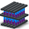
Fabrication and structural characterization of the 2 × 32 × 32 stacked memristor crossbar array. (a) Schematic illustration of the 3D stacked crossbar architecture. The MEs function as the TEs for the first-layer devices and simultaneously as the BEs for the second-layer devices, enabling the inherent current-subtraction pathway required for in-memory operations. (b) Process flow for fabricating the vertically stacked array. All steps for the second-layer crossbar are performed below 350 °C to preserve the characteristics of the first-layer devices. After patterning the first-layer BEs, the HfO₂/TiOₓ/TiOᵧ switching stack is deposited, followed by ME formation. A PECVD SiO₂ passivation layer is then deposited, vias are etched to expose the ME surfaces, and the second-layer device stack and TEs are subsequently formed. (c) Detailed cross-sectional device stack of both layers, consisting of Pt/HfO₂/TiOₓ/TiOᵧ/Pt. The two memristor layers share identical switching stacks and are electrically isolated using a SiO₂ layer. (d) Cross-sectional SEM image confirming complete vertical integration of the first- and second-layer crossbars, as well as the via connection enabling direct electrical contact to the shared ME. (e) Top-view optical microscope image of the fabricated 2 × 32 × 32 array, showing orthogonal routing of the BE/TE lines (horizontal) and ME lines (vertical) that form cross-point devices in both layers. The aligned via openings at BE–ME intersections ensure precise connectivity for the upper-layer devices. (Image: Reproduced with permission from Wiley-VCH Verlag) (click on image to enlarge)
The innovation exploits a shared middle electrode connecting two vertically stacked memristor layers. The lower layer stores weight values while the upper layer stores their squares. When input voltages are applied, currents flow through both layers simultaneously but with opposite polarity. The middle electrode naturally sums these opposing currents, yielding a net value proportional to squared Euclidean distance. The neuron producing the smallest current corresponds to the best matching unit.
The team fabricated a 2 × 32 × 32 stacked array using hafnium oxide and titanium oxide films between platinum electrodes. All second-layer fabrication stayed below 350 °C to avoid damaging underlying devices, maintaining compatibility with standard semiconductor manufacturing. Both layers exhibited forming-free operation, switching resistance states immediately without high-voltage pretreatment.
The devices achieved 32 distinct conductance levels with ±37.5 nS programming tolerance. Endurance testing confirmed stable switching over more than 10⁴ cycles, while retention measurements projected multi-year data stability at room temperature.
The subtraction mechanism performed accurately. Middle electrode currents tracked ideal values with a correlation coefficient of 0.96 and standard deviation of approximately 50 nA. This precision proved sufficient to reliably identify the best matching unit even under worst-case device variations.
Three tasks validated the architecture. First, the researchers tackled a ten-city traveling salesman problem using a ring-shaped self-organizing map with 64 nodes. Over 2000 training epochs, the network learned to order cities efficiently, reducing total tour distance from 4.71 to 3.50 in normalized units.
Second, the team clustered the Iris dataset, a benchmark containing 150 flower samples across three species described by four measurements each. An eight-by-eight neuron grid successfully separated the classes into three compact regions with minimal overlap.
Third, software-hardware co-simulation demonstrated image color quantization. A 512 × 512 pixel image underwent palette compression while preserving structural features, scoring well on standard quality metrics.
Across all tasks, hardware outputs closely matched ideal software simulations despite five-bit weight quantization and device variation of roughly 10%. The relative ordering of distances remained stable, ensuring correct best matching unit selection.
The architecture delivers inherent efficiency advantages. Vertical stacking roughly halves the footprint compared with planar designs requiring separate arrays. Parallel evaluation means computational energy scales weakly with input dimensionality, unlike digital processors that must execute separate operations for each dimension.
Challenges remain for scaling. Larger arrays will demand strategies to mitigate voltage drops and parasitic coupling. The current system uses a hybrid approach where weight updates are computed in software, leaving fully autonomous on-chip learning for future development.
The demonstrated system establishes that distance-based unsupervised learning can map efficiently onto memristive hardware through three-dimensional device engineering. The researchers suggest such hardware could function as a front-end module performing initial clustering before passing simplified data to downstream processors. For edge devices operating under strict power constraints, this combination of compact size, low energy consumption, and native support for unsupervised pattern discovery could prove particularly valuable.
For authors and communications departmentsclick to open
Lay summary
Prefilled posts
Nanowerk Newsletter
Get our Nanotechnology Spotlight updates to your inbox!
Thank you!
You have successfully joined our subscriber list.
Become a Spotlight guest author! Join our large and growing group of guest contributors. Have you just published a scientific paper or have other exciting developments to share with the nanotechnology community? Here is how to publish on nanowerk.com.