| Jan 23, 2026 |
Placing a thin layer of molybdenum disulfide on diamond enables current flow at room temperature, opening a new pathway for diamond-based electronic devices.
(Nanowerk News) Beyond the sparkle, diamonds have hidden talents. They shed heat better than any material, tolerate extreme temperatures and radiation and handle high voltages while wasting almost no electricity — ideal traits for compact, high-power devices.
|
|
These properties make diamond-based electronics promising for applications in the power grid, industrial power switches and places with high radiation, such as space or nuclear reactors. Diamond’s ability to quickly carry heat away from electronic components allows devices to handle large currents and voltages without overheating. This means smaller devices can be used to switch to high power in the grid or in industrial settings. Diamond’s natural resistance to radiation and extreme temperatures could enable electronics to work reliably in places where traditional silicon devices fail.
|
|
Researchers at Argonne National Laboratory are harnessing these strengths, not for jewelry, but as the foundation for powerful, next‑generation electronics (Nano Letters, “Heterogenous Integration of Boron-Doped p-Diamond with Monolayer n-MoS2 for PN Junctions Operating at Room Temperature”).
|
 |
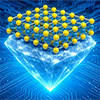
| Illustration showing two-dimensional molybdenum disulfide (yellow and blue spheres) stacked on diamond, a combination that helps electric current flow and could enable a new type of diamond-based electronics. (Image: Argonne National Laboratory)
|
|
However, despite all its advantages, diamond has yet to find widespread use in electronic devices. “Diamond hasn’t become a mainstream semiconductor material yet due to a few bottlenecks,” explained Argonne materials scientist Anirudha Sumant. “Most notable is the difficulty of n-type doping.”
|
|
N-type doping means adding a tiny amount of another element to the diamond crystal lattice, its internal scaffold. This supplies extra electrons for electrical conduction. In contrast, p‑type doping creates “holes” that act like positive charges. When an n-type region meets a p-type region, they form a PN junction — a one-way gate for electric current and the heart of devices like diodes and transistors.
|
|
“In microelectronics, you need a PN junction to make a device,” said Sumant. “Diamond has exceptional properties compared with other wide-bandgap materials, but efficient n-type doping at room temperature is a major problem.”
|
|
Wide-bandgap materials are special semiconductors that can handle more energy. This wider gap lets them work better at higher voltages and temperatures and in harsher environments than silicon-based electronics.
|
|
One way scientists have tried to dope diamond is by adding phosphorus. However, diamond lattice is very rigid, and phosphorus atoms are large. This causes strain and defects in the material. In diamond, phosphorus holds its extra electron so tightly that, at room temperature, there isn’t enough energy to free it. As a result, phosphorus‑doped diamond works well only at high temperatures, which limits its practical use.
|
|
Another promising approach to dope diamond is heterointegration: combining two different materials. With the rise of two-dimensional (2D) materials, like graphene, which are one atom thick, researchers have become interested in stacking these with bulk materials like diamond.
|
|
“I thought, why not integrate an n-type 2D material with p-type diamond? That could produce electrostatic doping and unlock interesting properties,” Sumant said.
|
|
Electrostatic doping is a way to change how a material conducts electricity without adding new atoms. Instead of mixing in chemical dopants, scientists use electric fields from a nearby layer or gate to “push” or “pull” electrons into the material. This creates regions that behave like n-type or p-type, but without permanently changing the material’s composition.
|
|
At the Center for Nanoscale Materials, a DOE Office of Science user facility at Argonne, Sumant and his team discovered that stacking a thin, 2D layer of molybdenum disulfide, a well-studied 2D material, on diamond created the right conditions for charges to move at the interface. This made the diamond act as if it had been doped, without the usual challenges of chemical doping.
|
|
With traditional doping, electrons are shared throughout the material. When voltage is applied, charges move and combine to create current. With heterointegration, something different happens. When a voltage is applied, electrons “tunnel” into the p-doped diamond, where they join with the holes.
|
|
“This tunneling helps electrons and holes come together to produce current, allowing the device to work at room temperature,” explained Akshay Wali, an Argonne post-doctoral fellow and lead author of a study describing these findings.
|
|
“Just by stacking a 2D material on diamond, we get performance numbers that haven’t been seen before in diamond-based devices,” Sumant added. “It’s a new way forward for electronics.”
|
|
Because diamond is naturally resistant to heat and radiation, it can help protect the ultrathin 2D layer. These devices may stay stable and reliable even under demanding conditions that challenge conventional electronics. This could make them well-suited for use in environments where there is high heat, strong electrical currents or radiation.
|
|
Looking ahead, the Argonne team plans to test these diamond-based devices for radiation hardness and compatibility with standard electronics. They are also exploring other 2D materials to further improve performance.
|