Researchers use circularly polarized light to control the direction of exciton polaritons in 2D semiconductors, enabling new tools for nanoscale photonics.
(Nanowerk Spotlight) Directing light along chosen paths with high spatial precision is a persistent challenge in photonics. Unlike electric charge, which can be guided using electric and magnetic fields, light lacks mass and is more difficult to confine and steer, especially at the nanoscale.
To develop photonic technologies capable of replacing or complementing electronic systems, researchers are turning to new forms of hybrid quasiparticles known as polaritons. These arise when photons couple strongly to matter excitations—such as excitons, which are bound electron–hole pairs in semiconductors. Polaritons can propagate in tightly confined modes, offering a route to efficient on-chip energy transport and optical signal processing beyond the limits of conventional optics.
Controlling the direction of polariton propagation is a key technical hurdle. Previous efforts have relied on structural asymmetries, external magnetic fields, or engineered gratings to impose directional behavior. These approaches add complexity and are not easily scalable. An alternative mechanism, inspired by principles from spintronics, uses spin–orbit coupling (SOC) to induce directionality.
In optical systems, SOC refers to the interaction between the spin of light—encoded in its polarization—and its momentum. When circularly polarized light interacts with certain nanostructures or material systems, it can preferentially launch guided modes that travel in one direction. This interaction does not require magnetic fields or broken structural symmetry, making it an attractive solution for integrated photonic circuits.
While the concept of SOC-driven directionality has been studied in plasmonic and valleytronic systems, directly imaging such effects at the nanoscale in real space has remained technically difficult. Detecting near-field guided modes, resolving their directionality, and linking this behavior to spin-dependent excitation requires both precise control over the light source and a method for capturing subwavelength optical fields. Until now, this combination has not been demonstrated for exciton polaritons in layered semiconductors.
A study published in Advanced Materials (“Direct Observation of Unidirectional Exciton Polaritons in Layered van der Waals Semiconductors”) presents the first direct real-space observation of unidirectional exciton polaritons in a two-dimensional material. The work, conducted by researchers at the University of Electronic Science and Technology of China and Nanyang Technological University, demonstrates how circularly polarized light can induce spin-controlled propagation of polaritons in tungsten disulfide (WS₂), a member of the transition metal dichalcogenide (TMD) family. This research introduces a method for launching and imaging polaritonic modes with directional selectivity determined purely by the polarization state of light.
Exciton polaritons in this context are formed in WS₂ flakes placed on a silicon dioxide substrate. These flakes support waveguide modes that strongly couple with excitons, leading to hybrid light–matter states that can travel tens of micrometers. The team used scattering-type scanning near-field optical microscopy (s-SNOM), a technique in which a sharp atomic force microscope (AFM) tip is illuminated by a laser beam to generate localized optical excitations.
By focusing a circularly polarized laser at the AFM tip, they created a nanoscale dipole source with both vertical and horizontal field components. This dipole mimics the behavior of a spinning emitter and launches waveguided polaritons whose direction depends on the helicity of the light.
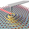
Spin-controlled excitation of guided polaritons in a layered semiconductor. A circularly polarized laser beam is directed at an atomic force microscope (AFM) tip above a thin WS₂ flake. This setup creates a nanoscale rotating dipole that launches hybrid light–matter waves, called exciton polaritons, into the flake. (a) Schematic showing how the circular polarization and spin–orbit interaction result in asymmetric polariton propagation. (b) As the WS₂ thickness increases, both transverse electric (TE) and transverse magnetic (TM) waveguide modes appear, each with different wavevectors. (c, d) Simulations of TE₀ modes in a thin (10 nm) WS₂ flake show that the field distribution is symmetric for both left- and right-circularly polarized dipoles. (e, f) In a thicker (62 nm) flake supporting TM₀ modes, the field distribution becomes strongly asymmetric, with the propagation direction depending on the light’s polarization. (g) The directionality ratio R quantifies how strongly the wave travels in one direction compared to the other, depending on the polarization state. The maximum asymmetry occurs for TM modes at higher in-plane momentum. The inset shows how the circular polarization at the tip can be broken into horizontal and vertical components, leading to elliptically polarized dipoles that excite the waveguide. (Image: reprinted with permission by Wiley-VCH Verlag) (click on image to enlarge)
The key insight is that the layered structure of WS₂ supports different types of guided modes: transverse electric (TE) modes, where the electric field lies in the plane of the material, and transverse magnetic (TM) modes, which include strong out-of-plane components. The TE modes serve as a useful reference because they propagate symmetrically regardless of polarization.
By contrast, TM modes show asymmetric propagation when excited with left- versus right-circularly polarized light. This asymmetry arises from the SOC-induced coupling between the dipole field and the waveguide modes.
The researchers examined how this behavior depends on the thickness of the WS₂ flakes. In thin flakes, around 7–10 nanometers, only the fundamental TE mode is supported. Imaging these modes under opposite circular polarizations yielded identical interference patterns, confirming their symmetry and providing a baseline for calibration. In thicker flakes, up to 125 nanometers, higher-order TM modes become available. These exhibit pronounced directionality. When the incident light was left-circularly polarized, the TM polariton wave propagated strongly in one direction; when the polarization was reversed, the propagation direction flipped.
To quantify the directionality, the team calculated the unidirectionality ratio, defined as the ratio of spectral amplitudes for oppositely polarized illumination. For the lowest-order TM mode in a 125 nm flake, the ratio reached 0.291. This value indicates a more than threefold difference in propagation strength depending on polarization. This measurement was made by performing a Fourier transform on the near-field images to analyze the wavevector components. TE modes showed no such variation, reinforcing that the observed asymmetry is due to SOC effects specific to TM polaritons.
The theoretical foundation for this behavior lies in the decomposition of the dipole field into spatial frequency components. For TM modes, the vertical component of the dipole field couples more efficiently to one direction in the waveguide, depending on the sign of the circular polarization. This results in an asymmetric distribution of wavevectors in momentum space, which is directly visible in the experimental data.
Numerical simulations support this interpretation, showing that thicker WS₂ flakes support more confined TM modes with higher wavevectors, and that the degree of unidirectionality increases with confinement.
To ensure that observed differences were not due to variations in the experimental setup—such as differences in tip response or laser intensity—the researchers used the symmetric TE mode as a built-in calibration. Since TE excitation is insensitive to polarization handedness, any measured difference in its spectral amplitude between left and right circular polarization was used as a normalization factor. This method allowed the team to isolate genuine SOC-induced effects from artifacts.
Further experiments showed that higher-order TM modes, such as TM₁, could also be excited in thick flakes. These modes, while less confined than TM₀, coupled more efficiently to the AFM tip due to their spatial field distribution. As a result, they appeared more prominently in the measured signal, even though their directionality was lower. The contrast in signal strength between TM₀ and TM₁ modes was explained by a combination of field overlap and propagation characteristics, all consistent with the theoretical models.
This work provides both a demonstration and a practical methodology for visualizing spin-controlled propagation of light–matter waves in two-dimensional materials. By showing that circular polarization alone can determine the direction of polariton flow, the study opens a path toward photonic components that route optical signals based on spin. Such components could be integrated into nanoscale devices for optical computing, communication, or quantum information systems. The results also offer a framework for exploring SOC effects in other polaritonic systems, including those based on different TMDs or dielectric heterostructures.
The combination of near-field imaging, polarization control, and analytical modeling presented here makes it possible to directly measure how spin and momentum interact in confined light systems. The approach offers a new toolset for investigating and engineering light–matter interactions at the nanoscale, with potential applications in ultracompact photonic circuits where precise control of optical directionality is required.
Get our Nanotechnology Spotlight updates to your inbox!
Thank you!
You have successfully joined our subscriber list.
Become a Spotlight guest author! Join our large and growing group of guest contributors. Have you just published a scientific paper or have other exciting developments to share with the nanotechnology community? Here is how to publish on nanowerk.com.