| Jan 22, 2026 |
Parallel piezo aligners with fly height sensors enable faster PIC wafer testing.
(Nanowerk News) PI (Physik Instrumente) announced a new technology platform for electro-optical wafer-level testing designed to validate electrical and optical device functions simultaneously in high-volume production. The system combines high-density electrical probing with automated photonic alignment in a compact architecture built for ATE compatibility.
|
 |
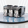
| Parallel miniaturized piezoelectric alignment engines with fly-height sensors enable faster PIC wafer testing. (Image: PI)
|
Parallel Operation and Scalability
|
|
Designed for production scale, the platform supports parallel operation of multiple miniaturized alignment engines across a single wafer, enabling simultaneous electro-optical probing at multiple test sites to increase throughput and lower cost of test. Its compact, ATE-compatible architecture is intended to make it practical to deploy many aligners in one setup—helping EPIC manufacturers transition from sequential, lab-style alignment to high-volume, repeatable wafer-level testing.
|
|
A key new feature is FAU ranging, an interferometry-based fly-height measurement method that uses existing fiber channels—adding no extra hardware and no additional footprint—to measure fiber-to-wafer distance at the point of interest, supporting stable probing and repeatable optical coupling. PI notes that FAU ranging can also enable future approaches such as trench-based photonic edge coupling, helping save wafer real estate and reduce device costs.
|
|
“With FAU ranging, we pave the way for trench-based photonic edge coupling, saving wafer real estate, reducing device costs, and unlocking new design freedom for EPIC manufacturers.,” says Dr. Markus Simon, Strategic Innovation and Technology Management at PI.
|
|
PI will present the platform at SPIE Photonics West 2026.
|
Industries Served
|
|
Photonics, electro-optical wafer testing.
|


