| May 06, 2025 |
Researchers have used laser light to draw electronic circuits directly onto flexible films, sculpting 2D materials without chemicals, photolithography, or cleanrooms.
|
|
(Nanowerk Spotlight) What if you could draw a working electronic circuit—right onto a flexible, transparent film—using just a beam of light?
|
|
That’s precisely what researchers at the Instituto de Ciencia de Materiales de Madrid (ICMM-CSIC) and the Universidad Politécnica de Madrid (UPM) have accomplished. Led by PhD student Yiğit Sözen and Professor Andrés Castellanos-Gómez, the team developed a laser-based method to directly sculpt high-performance electronics from atomically thin 2D materials—no photolithography, chemicals, or cleanrooms required.
|
|
The concept builds on a high-throughput technique known as roll-to-roll exfoliation, used to deposit large-area films of 2D materials like graphite and transition metal dichalcogenides (TMDs). The new twist? A pulsed infrared laser precisely removes regions of the film, patterning circuits directly onto flexible substrates such as polycarbonate.
|
|
“We were amazed by how well it worked from the start,” Castellanos-Gómez said. “This was one of those rare experiments that just clicked right away.”
|
|
The team originally used visible lasers to modify MoS₂ but found that other materials like graphite were too resilient. Switching to an infrared pulsed laser—commonly used in their lab for metal engraving—unlocked the ability to cleanly ablate a wide variety of 2D materials with micrometer resolution.
|
|
By skipping traditional lithographic steps, the technique makes rapid prototyping not only possible but effortless. “We’re already using this every day in the lab,” Sözen said. “It saves us so much time when building flexible devices.”
|
 |
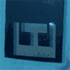
| Figure 1. Composite image illustrating the laser ablation process used to pattern interdigitated electrodes on a roll-to-roll exfoliated graphite film deposited on a flexible polycarbonate substrate. (Image courtesy of the researchers)
|
|
In a striking proof-of-concept, they used the method to fabricate interdigitated graphite electrodes—a common architecture in supercapacitors and chemical sensors. Collaborators Javier Martinez and Yu Kyoung Ryu at UPM helped validate these structures as functioning micro-supercapacitors, expanding the method’s potential well beyond simple circuits.
|
|
But the most thrilling moment? “When we fabricated a pixelated photodetector array using only 2D materials and the laser, we realized we had made a real camera,” Castellanos-Gómez shared. “It was a first for our lab, and it showed how powerful this approach could be.”
|
 |
| Figure 2. Composite image depicting the fabrication process of a WSe₂/graphite photodetector array, highlighting the transfer of laser-patterned WSe₂ film onto laser-patterned graphite pads on a polycarbonate substrate. (Image courtesy of the researchers)
|
|
That device, a hybrid of graphite electrodes and WSe₂, successfully captured light patterns with high sensitivity and uniformity, all while being semi-transparent and bendable—hinting at future uses in wearables, smart windows, and lightweight imaging systems.
|
|
The team is now preparing to integrate the laser setup directly into their roll-to-roll system, waiting on a new laser model that will synchronize beam scanning with moving substrates. This could unlock industrial-scale production of flexible electronics based solely on van der Waals materials.
|
|
Published in Advanced Functional Materials (“Direct Laser Ablation of 2D Material Films for Fabricating Multi-Functional Flexible and Transparent Devices”), this open-access study signals a major step toward simpler, cleaner, and more scalable electronics manufacturing (see also this related earlier work in Small Methods: “High-throughput mechanical exfoliation for low-cost production of van der Waals nanosheets”).
|
|
Provided by the Instituto de Ciencia de los Materiales de Madrid
|
|
|