A security device made from gold nanoparticles uses light alone to create, verify, and reset uncopyable identities, enabling repeated defense against counterfeiting.
(Nanowerk Spotlight) Every counterfeit microchip that slips into a military aircraft or medical device represents a potentially catastrophic failure. The global counterfeiting problem costs industries hundreds of billions of dollars annually, but the deeper threat is one of trust: how can a manufacturer, distributor, or end user verify that a component is genuine?
Traditional security measures like holograms and serial numbers can be copied. Digital cryptographic keys, stored in memory, can be extracted. In the early 2000s, a fundamentally different approach emerged from MIT, where researcher Ravindra Pappu proposed what he called a physical one-way function (Science, 2002, DOI: 10.1126/science.1074376). The idea was to exploit the random microscopic structure of a physical object as an uncopyable identifier, much like a fingerprint.
This concept evolved into what the field now calls the physical unclonable function, or PUF: a device whose inherent physical randomness generates unique, unpredictable responses when probed with a specific stimulus.
PUFs have since branched into two main families. Electrical PUFs use circuit-level variations to produce electronic signatures, making them easy to embed in chips but sometimes vulnerable to machine-learning algorithms that can learn to predict their outputs. Optical PUFs use light-based signals and tend to generate far more complex responses drawn from richer sources of randomness.
Yet both types share a fundamental weakness. Once an attacker captures enough of a PUF’s responses, or physically accesses the device itself, the security is permanently broken. The underlying structure does not change, so the compromise cannot be undone. Replacing the PUF means replacing hardware, which is costly and impractical at scale.
Several research groups have attempted to solve this by building reconfigurable optical PUFs whose physical structure can be altered on demand to restore security. These efforts have relied on thermal treatments, such as recrystallizing salt solutions or triggering phase changes in liquid crystals with heat.
While promising in laboratory demonstrations, thermal methods face a practical dilemma: low-temperature reconfiguration risks accidental changes during normal use, while high-temperature processing can damage the electronic systems the PUF is supposed to protect.
A study published in Advanced Materials (“All‐Optical Reconfigurable Physical Unclonable Function for Sustainable Security”) offers a way around this problem. A research team at Sungkyunkwan University in South Korea has developed a PUF system that uses only light for every stage of its lifecycle: fabrication, readout, and reconfiguration. No heat treatment is required at any point.
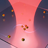
Optical nanopatterning via sintering of AuNPs using an optical tweezer system. (a) Schematic illustration of the nanopatterning process. (b) Dark-field microscopy (DFM) image of patterned 44 AuNPs, representing the letters ‘N, A, N, O’ as dots. (c) DFM images and time-resolved optical scattering spectra during the nanopatterning process. (Image: Reproduced with permission from Wiley-VCH Verlag) (click on image to enlarge)
The system starts with gold nanoparticles, each roughly 100 nm across, suspended in water above a glass substrate. A tightly focused infrared laser operating at 980 nm acts as an optical tweezer, trapping individual particles near the glass surface. The particles jiggle randomly due to Brownian motion, the thermal agitation that causes microscopic objects in liquid to wander unpredictably.
When two or more trapped particles drift close enough together, an electromagnetic effect called plasmonic coupling concentrates intense heat in the narrow gap between them. This localized heating fuses the particles into a single, larger, highly spherical gold nanoparticle within nanoseconds to microseconds. The fused particle then adheres to the glass through van der Waals attraction, a weak but sufficient molecular force.
The security value of this process lies in its randomness. Because Brownian motion governs when and where particles meet, fuse, and settle, no two patterns are alike. The fused particles also scatter light differently depending on how many original particles merged and at what orientations. A particle formed from two precursors scatters at a different peak wavelength than one formed from three or four. This creates what the researchers term spatiospectral complexity: randomness encoded simultaneously in each particle’s position and its optical signature.
To make the technique viable for manufacturing, the team developed a laser-writing method in which the optical trap glides continuously across the substrate, depositing particles along programmable paths. A scan speed of 0.25 µm/s produced the best balance between pattern density and fabrication reliability, with each 18 µm pattern taking about 72 s to write. The method works on multiple substrate materials, including aluminum oxide and polyethylene terephthalate, without causing damage.
From each pattern’s light-scattering response, the researchers extracted a 384-bit security key. The key-generation process compresses spectral data into a 64-element vector, sorts the values, and converts the resulting rank order into binary code. This scheme inherently produces equal frequencies of zeros and ones, a property that maximizes entropy and strengthens cryptographic quality.
The team evaluated 75 PUF devices through a comprehensive suite of security tests. Shannon entropy, a standard measure of information content, remained near the theoretical maximum across all key segments. The keys passed the National Institute of Standards and Technology randomness test suite at rates matching those of a standard cryptographic random-number generator. Hamming distances between different devices, a measure of how many bits differ between two keys, clustered tightly around the ideal value of 0.5, confirming that each device produces a distinct identity.
Four machine-learning algorithms trained to predict unknown portions of the keys performed no better than random guessing. The estimated probability of successfully cloning a key was approximately 8.61 × 10⁻³⁰, and the encoding density reached about 5.24 µm⁻², among the highest reported for optical PUFs.
The researchers also demonstrated a lightweight authentication protocol suitable for supply-chain traceability. Using exclusive-OR masking and Hamming-distance verification, the system maintained a zero false-positive rate across a wide threshold range.
The central advance, however, is the reconfiguration mechanism. By scanning a fabricated PUF with a focused 532 nm laser while the pattern sits beneath a thin layer of silicone-based fluid (polydimethylsiloxane), the researchers trigger localized heating that causes the fluid to expand thermally. This expansion nudges the gold nanoparticles into new positions, a process the authors call optothermal nudging.
The rearrangement is irreversible and unpredictable: individual particles follow diverse, non-repeating trajectories, and some nanoparticle clusters split apart or change shape entirely.
After reconfiguration, each PUF generates keys that are statistically independent from its previous keys, as confirmed by mutual-information analysis. Across 20 devices subjected to four successive reconfigurations, every reconfigured key was clearly distinguishable from prior keys and from those of all other devices. Security metrics, including NIST randomness tests, remained consistently strong after each cycle.
The approach does require microscopic optical equipment for readout, which limits consumer-facing applications. But industries that most urgently need component-level authentication, including semiconductor manufacturing, aerospace, defense, and biomedical device production, already operate this kind of inspection infrastructure routinely. The independent, localized nature of the patterning process also opens a path toward parallel fabrication using holographic optical-tweezer systems, which could increase throughput substantially.
What distinguishes this work is its architectural coherence. A single optical platform handles fabrication, verification, and renewal, with no thermal processing, no physical contact, and no hardware replacement. In security applications where static defenses inevitably erode as attackers grow more sophisticated, the ability to regenerate a device’s identity on demand while preserving its proven security properties addresses a concrete and previously unresolved vulnerability in optical PUF technology.
For authors and communications departmentsclick to open
Lay summary
Prefilled posts
Nanowerk Newsletter
Get our Nanotechnology Spotlight updates to your inbox!
Thank you!
You have successfully joined our subscriber list.
Become a Spotlight guest author! Join our large and growing group of guest contributors. Have you just published a scientific paper or have other exciting developments to share with the nanotechnology community? Here is how to publish on nanowerk.com.
A security device made from gold nanoparticles uses light alone to create, verify, and reset uncopyable identities, enabling repeated defense against counterfeiting.
(Nanowerk Spotlight) Every counterfeit microchip that slips into a military aircraft or medical device represents a potentially catastrophic failure. The global counterfeiting problem costs industries hundreds of billions of dollars annually, but the deeper threat is one of trust: how can a manufacturer, distributor, or end user verify that a component is genuine?
Traditional security measures like holograms and serial numbers can be copied. Digital cryptographic keys, stored in memory, can be extracted. In the early 2000s, a fundamentally different approach emerged from MIT, where researcher Ravindra Pappu proposed what he called a physical one-way function (Science, 2002, DOI: 10.1126/science.1074376). The idea was to exploit the random microscopic structure of a physical object as an uncopyable identifier, much like a fingerprint.
This concept evolved into what the field now calls the physical unclonable function, or PUF: a device whose inherent physical randomness generates unique, unpredictable responses when probed with a specific stimulus.
PUFs have since branched into two main families. Electrical PUFs use circuit-level variations to produce electronic signatures, making them easy to embed in chips but sometimes vulnerable to machine-learning algorithms that can learn to predict their outputs. Optical PUFs use light-based signals and tend to generate far more complex responses drawn from richer sources of randomness.
Yet both types share a fundamental weakness. Once an attacker captures enough of a PUF’s responses, or physically accesses the device itself, the security is permanently broken. The underlying structure does not change, so the compromise cannot be undone. Replacing the PUF means replacing hardware, which is costly and impractical at scale.
Several research groups have attempted to solve this by building reconfigurable optical PUFs whose physical structure can be altered on demand to restore security. These efforts have relied on thermal treatments, such as recrystallizing salt solutions or triggering phase changes in liquid crystals with heat.
While promising in laboratory demonstrations, thermal methods face a practical dilemma: low-temperature reconfiguration risks accidental changes during normal use, while high-temperature processing can damage the electronic systems the PUF is supposed to protect.
A study published in Advanced Materials (“All‐Optical Reconfigurable Physical Unclonable Function for Sustainable Security”) offers a way around this problem. A research team at Sungkyunkwan University in South Korea has developed a PUF system that uses only light for every stage of its lifecycle: fabrication, readout, and reconfiguration. No heat treatment is required at any point.
Optical nanopatterning via sintering of AuNPs using an optical tweezer system. (a) Schematic illustration of the nanopatterning process. (b) Dark-field microscopy (DFM) image of patterned 44 AuNPs, representing the letters ‘N, A, N, O’ as dots. (c) DFM images and time-resolved optical scattering spectra during the nanopatterning process. (Image: Reproduced with permission from Wiley-VCH Verlag) (click on image to enlarge)
The system starts with gold nanoparticles, each roughly 100 nm across, suspended in water above a glass substrate. A tightly focused infrared laser operating at 980 nm acts as an optical tweezer, trapping individual particles near the glass surface. The particles jiggle randomly due to Brownian motion, the thermal agitation that causes microscopic objects in liquid to wander unpredictably.
When two or more trapped particles drift close enough together, an electromagnetic effect called plasmonic coupling concentrates intense heat in the narrow gap between them. This localized heating fuses the particles into a single, larger, highly spherical gold nanoparticle within nanoseconds to microseconds. The fused particle then adheres to the glass through van der Waals attraction, a weak but sufficient molecular force.
The security value of this process lies in its randomness. Because Brownian motion governs when and where particles meet, fuse, and settle, no two patterns are alike. The fused particles also scatter light differently depending on how many original particles merged and at what orientations. A particle formed from two precursors scatters at a different peak wavelength than one formed from three or four. This creates what the researchers term spatiospectral complexity: randomness encoded simultaneously in each particle’s position and its optical signature.
To make the technique viable for manufacturing, the team developed a laser-writing method in which the optical trap glides continuously across the substrate, depositing particles along programmable paths. A scan speed of 0.25 µm/s produced the best balance between pattern density and fabrication reliability, with each 18 µm pattern taking about 72 s to write. The method works on multiple substrate materials, including aluminum oxide and polyethylene terephthalate, without causing damage.
From each pattern’s light-scattering response, the researchers extracted a 384-bit security key. The key-generation process compresses spectral data into a 64-element vector, sorts the values, and converts the resulting rank order into binary code. This scheme inherently produces equal frequencies of zeros and ones, a property that maximizes entropy and strengthens cryptographic quality.
The team evaluated 75 PUF devices through a comprehensive suite of security tests. Shannon entropy, a standard measure of information content, remained near the theoretical maximum across all key segments. The keys passed the National Institute of Standards and Technology randomness test suite at rates matching those of a standard cryptographic random-number generator. Hamming distances between different devices, a measure of how many bits differ between two keys, clustered tightly around the ideal value of 0.5, confirming that each device produces a distinct identity.
Four machine-learning algorithms trained to predict unknown portions of the keys performed no better than random guessing. The estimated probability of successfully cloning a key was approximately 8.61 × 10⁻³⁰, and the encoding density reached about 5.24 µm⁻², among the highest reported for optical PUFs.
The researchers also demonstrated a lightweight authentication protocol suitable for supply-chain traceability. Using exclusive-OR masking and Hamming-distance verification, the system maintained a zero false-positive rate across a wide threshold range.
The central advance, however, is the reconfiguration mechanism. By scanning a fabricated PUF with a focused 532 nm laser while the pattern sits beneath a thin layer of silicone-based fluid (polydimethylsiloxane), the researchers trigger localized heating that causes the fluid to expand thermally. This expansion nudges the gold nanoparticles into new positions, a process the authors call optothermal nudging.
The rearrangement is irreversible and unpredictable: individual particles follow diverse, non-repeating trajectories, and some nanoparticle clusters split apart or change shape entirely.
After reconfiguration, each PUF generates keys that are statistically independent from its previous keys, as confirmed by mutual-information analysis. Across 20 devices subjected to four successive reconfigurations, every reconfigured key was clearly distinguishable from prior keys and from those of all other devices. Security metrics, including NIST randomness tests, remained consistently strong after each cycle.
The approach does require microscopic optical equipment for readout, which limits consumer-facing applications. But industries that most urgently need component-level authentication, including semiconductor manufacturing, aerospace, defense, and biomedical device production, already operate this kind of inspection infrastructure routinely. The independent, localized nature of the patterning process also opens a path toward parallel fabrication using holographic optical-tweezer systems, which could increase throughput substantially.
What distinguishes this work is its architectural coherence. A single optical platform handles fabrication, verification, and renewal, with no thermal processing, no physical contact, and no hardware replacement. In security applications where static defenses inevitably erode as attackers grow more sophisticated, the ability to regenerate a device’s identity on demand while preserving its proven security properties addresses a concrete and previously unresolved vulnerability in optical PUF technology.
For authors and communications departmentsclick to open
Lay summary
Prefilled posts
Nanowerk Newsletter
Get our Nanotechnology Spotlight updates to your inbox!
Thank you!
You have successfully joined our subscriber list.
Become a Spotlight guest author! Join our large and growing group of guest contributors. Have you just published a scientific paper or have other exciting developments to share with the nanotechnology community? Here is how to publish on nanowerk.com.