| Jan 29, 2026 |
A flexible photodetector using asymmetric 2D heterostructures switches spectral response by gate voltage, enabling filter-free wavelength control under bending.
(Nanowerk News) Flexible photodetectors are increasingly required in applications such as wearable health monitoring, curved imaging systems, and soft optoelectronic interfaces, where both mechanical compliance and spectral discrimination are critical. Conventional rigid photodetectors struggle under deformation, while most flexible alternatives depend on external filters or complex optical components to achieve wavelength selectivity. These approaches increase device thickness, limit integration, and reduce optical efficiency.
|
|
Although two-dimensional materials provide tunable electronic structures and strong light–matter interactions, their potential for electrically controlled spectral differentiation has remained largely unexplored. Based on these challenges, it is necessary to conduct in-depth research into intrinsically wavelength-selective, electrically tunable photodetectors suitable for flexible systems.
|
|
In a study published in Microsystems & Nanoengineering (“Gate-tunable flexible photodetector with wavelength-selective response based on asymmetric 2D heterostructures”), researchers from Xi’an Jiaotong University report a gate-tunable flexible photodetector built from asymmetric van der Waals heterostructures composed of graphene, molybdenum disulfide, and single-walled carbon nanotubes. The device is fabricated on a flexible polymer substrate and uses electrical gating to dynamically control carrier injection and transport. As a result, the photodetector can switch its peak photoresponse between different visible wavelengths while maintaining stable performance under mechanical bending.
|
 |
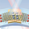
| Structure and characterization of the gate-tunable flexible photodetector based on Gr/MoS2/SWCNT asymmetric heterostructure. a Schematic of the 3D structure of the flexible photodetector based on Gr/MoS2/SWCNT. b Schematic of the working principle of the flexible photodetector based on Gr/MoS2/SWCNT. c Photograph of the flexible photodetector based on PET substrate. d SEM image of the flexible photodetector based on Gr/MoS2/SWCNT. e Comparison of Raman spectra of the flexible photodetector based on Gr/MoS2/SWCNT and the original MoS2 film. f Comparison enlarged diagram of MoS2 peak. (Image: Reproduced from DOI:10.1038/s41378-025-01109-9, CC BY) (click on image to enlarge)
|
|
The core innovation lies in the asymmetric design of the heterojunctions formed at opposite ends of the MoS₂ channel. Graphene–MoS₂ and carbon-nanotube–MoS₂ interfaces possess different work-function offsets, creating unequal built-in electric fields. This asymmetry establishes an internal potential gradient that effectively blocks thermally excited carriers under low bias, leading to strong dark-current suppression. Compared with symmetric devices, the asymmetric architecture improves specific detectivity by nearly an order of magnitude.
|
|
Crucially, the device’s spectral response is governed by gate voltage. By shifting the Fermi level of MoS₂, the applied gate voltage alters which heterojunction dominates photocarrier separation. Under positive gate bias, the graphene–MoS₂ junction is strengthened, enhancing responsivity at shorter wavelengths around 450 nm. Under negative gate bias, the MoS₂–nanotube junction becomes dominant, selectively amplifying longer-wavelength response near 635 nm. The device achieves responsivities up to 40.3 A/W and a maximum specific detectivity of 1.3 × 10¹¹ Jones.
|
|
Mechanical tests show that these optoelectronic characteristics remain stable under repeated bending, confirming that wavelength selectivity, sensitivity, and flexibility can coexist in a single electrically reconfigurable platform.
|
|
According to the researchers, the key advance is demonstrating that wavelength selectivity does not require additional optical components. By leveraging asymmetric interfacial band engineering, the device redistributes photogenerated carriers using only an external gate voltage. This approach not only simplifies device architecture but also allows real-time spectral reconfiguration. The team notes that such electrically controlled selectivity could be extended to broader wavelength ranges by integrating other two-dimensional semiconductors, offering a versatile strategy for next-generation flexible optoelectronic systems.
|
|
Electrically tunable, wavelength-selective photodetectors could significantly impact wearable sensing, environmental monitoring, optical communication, and compact imaging technologies. Eliminating external filters reduces system complexity, thickness, and optical loss, enabling tighter integration with flexible electronics and bio-integrated platforms.
|
|
The demonstrated gate-controlled spectral switching also opens opportunities for adaptive multispectral detection, where a single pixel can perform multiple sensing functions. More broadly, the asymmetric heterostructure strategy provides a design framework for developing reconfigurable optoelectronic devices that combine flexibility, high sensitivity, and spectral intelligence in a scalable format.
|