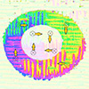
Spiral scanning creates six distinguishable polarization patterns in ferroelectric films, enabling data storage beyond binary and more than doubling information density per storage element.
(Nanowerk Spotlight) In 1971, Intel’s first commercial microprocessor contained 2,300 transistors. NVIDIA’s Blackwell B200, the processor powering the company’s latest artificial intelligence accelerators, contains 208 billion. This relentless miniaturization has powered five decades of computing progress, but it now approaches physical limits. Transistors measure just a few nanometers across, scales where quantum effects and manufacturing tolerances erect fundamental barriers.
Storage technology confronts similar constraints. Hard drives and flash memory have squeezed ever more bits into shrinking areas through continual refinement of one basic principle: encode information as one of two states. A magnetic domain points up or down. A charge sits trapped or absent. Binary logic. One or zero. Nothing in between.
But what if each storage element could reliably hold more than two distinguishable states? The arithmetic is seductive. Six states per element stores 2.6 times more information than binary in the same physical space. Eight states triples capacity. Sixteen quadruples it. The concept has attracted researchers for decades, yet practical implementation has proven elusive. Creating physically distinct states at the nanoscale presents one obstacle. Reading them back accurately poses another. Ensuring they remain stable for years without degradation presents yet another. Most proposed schemes have stumbled on at least one of these requirements.
Ferroelectric materials have drawn particular interest because their atomic structure naturally supports multiple polarization directions. In these crystalline substances, certain atoms settle into stable off-center positions, creating what physicists call an electric dipole: a persistent separation of positive and negative charge that points in a defined direction like a tiny, embedded arrow. This polarization remains fixed without power and switches when voltage is applied.
Some ferroelectrics go further, forming exotic arrangements called topological structures, where polarization vectors curl into vortices, twist into three-dimensional skyrmions, or interlock in patterns called closure domains. Each distinct configuration could theoretically represent a different data symbol.
Creating such structures in the laboratory has never been the problem. Researchers have produced them through elaborate thin-film growth on specially matched substrates, careful temperature cycling, or electrode geometries that constrain device design. The difficulty has been doing so practically. Reading nanoscale polarization patterns typically demanded electron microscopy or similar techniques, too slow and often destructive for functional memory. The structures remained scientific curiosities without clear paths toward application.
A study published in ACS Nano (“Autonomous Multistate Nanoencoding Using Combinatorial Ferroelectric Closure Domains in BiFeO3“) demonstrates a more viable approach. Researchers report writing and reading six distinct topological polarization states in bismuth ferrite (BiFeO₃) thin films using only an atomic force microscope tip tracing programmable spiral paths while applying voltage. No patterned top electrodes. No multilayer heterostructures. No temperature protocols. The tip spirals across the surface at −8 V bias, and the ferroelectric film organizes into a four-quadrant closure domain: a structure where polarization stripes alternate direction within each quadrant while the overall pattern forms a closed loop, like a nanoscale pinwheel.
Writing and reading striped closure domains in BFO. (a) Scan path was followed during writing; tip bias was −6 V. (b) Topography of the written structure. (c) X component of the polarization (inset shows Vero spot positions 1 and 2). (d) Y component of the polarization (inset shows Vero spot positions 3 and 4). (e) Z component of the polarization obtained through the average of the 1 and 2 positions. (f) 3D Vector PFM of the structure. α represents the angle of the polarization vector within the XY plane (color). β represents the angle of the polarization vector with respect to the Z-axis (transparency). (g) 3D arrow reconstruction. (h) SHG map of the same structure with a polarizer along the X-axis. (i) SHG map of the same structure with polarizer along the Y-axis. (j) Domain walls are j within the X direction. (k) Domain walls within the Y direction. (l) Domain walls within the Z direction. XY scale bar is 1 μm. (Image: Reproduced with permission from American Chemical Society) (click on image to enlarge)
BiFeO₃ enables this because of its unusual crystallography. The material belongs to a rare class called multiferroics, exhibiting both ferroelectric and magnetic order at room temperature. Its crystal structure supports eight distinct polarization directions, each containing both in-plane and out-of-plane components. This multiplicity provides raw material for engineering varied domain configurations through controlled switching sequences.
The researchers discovered striking tunability in their spiral-written structures. Adjusting spiral size scaled the closure domains from 1.4 μm down to 200 nm in radius while maintaining stability, approaching dimensions relevant to commercial memory. Varying the number of spiral turns altered pattern complexity. Reversing spiral direction, clockwise versus counterclockwise, produced closure domains with opposite handedness, a property physicists call chirality.
This sensitivity to scan direction, not observed in similar experiments on other ferroelectrics, suggests the switching mechanism in BiFeO₃ differs fundamentally from simpler materials. Writing nested spirals with opposite voltage polarity generated concentric structures, one closure domain embedded inside another.
These variables yielded six distinguishable configurations: two single spirals of opposite chirality plus four nested combinations varying inner and outer handedness. The team programmed their microscope to accept text input, convert characters to base-6 representation, and automatically write the corresponding topological symbols. They encoded “ORNL” in both binary and base-6 formats. Binary required 28 elements in a 4×7 grid. Base-6 needed only 12 elements in a 4×3 grid, more than doubling information density.
Reading these patterns required measuring complete three-dimensional polarization at each point. The researchers employed interferometric piezoresponse force microscopy, positioning a laser at four locations around the probe tip and detecting the sample’s mechanical vibration response to applied voltage.
Mathematical combination of these four signals reconstructed full polarization vectors across the scanned region. Second harmonic generation microscopy, an optical technique sensitive to crystalline symmetry breaking, independently confirmed the closure domain structures.
For automated symbol recognition, the team trained a machine learning classifier on 30 experimental patterns, five per symbol. After data augmentation and reserving 20% for testing, the classifier distinguished the six topological states with 99.6% accuracy.
The demonstration achieved an information density of approximately 10⁻⁶ bit/nm², about 100 times below commercial hard drives at roughly 10⁻⁴ bit/nm². Yet calculations indicate that shrinking structures below 140 nm diameter while expanding the alphabet to eight symbols would match current hard drive performance. Phase-field simulations confirmed these domain configurations are thermodynamically stable.
Repeated imaging over 1 month verified retention without degradation, demonstrating the nonvolatility that distinguishes ferroelectric storage from memory types like DRAM that require constant power to maintain data.
Formidable challenges separate this demonstration from practical technology. Both writing and reading depend on scanning probe microscopy, an inherently serial process vastly slower than electronic access in commercial memory. The researchers suggest alternatives that might accelerate readout: magnetic detection using nitrogen-vacancy center sensors or optical techniques exploiting structural chirality. They also demonstrated purely mechanical erasure, pressing the probe firmly without voltage to reset written patterns.
This work transforms a materials physics phenomenon into a functional encoding scheme. By automating both writing and recognition, the researchers establish that topological ferroelectric structures can serve as distinguishable symbols beyond binary. The approach exploits polarization complexity rather than avoiding it, converting BiFeO₃’s multiple accessible domain states into an expanded information alphabet. Competitive speeds and densities remain distant goals, but the demonstration provides concrete evidence that multistate ferroelectric memory, an idea with decades of theoretical appeal, can actually function.
For authors and communications departmentsclick to open
Lay summary
Prefilled posts
Nanowerk Newsletter
Get our Nanotechnology Spotlight updates to your inbox!
Thank you!
You have successfully joined our subscriber list.
Become a Spotlight guest author! Join our large and growing group of guest contributors. Have you just published a scientific paper or have other exciting developments to share with the nanotechnology community? Here is how to publish on nanowerk.com.