Researchers use DNA to assemble mixed-dimensional nanostructures with tunable optical properties, enabling scalable photodetectors with high sensitivity.
(Nanowerk Spotlight) Efforts to build high-performance optoelectronic devices have repeatedly run into the limitations of individual low-dimensional materials. Nanoparticles are excellent at absorbing and emitting light but suffer from poor charge transport. In contrast, two-dimensional (2D) semiconductors such as molybdenum disulfide (MoS₂) can move charge efficiently but interact less effectively with light.
Researchers have explored ways to combine these materials into mixed-dimensional heterostructures that could harness the advantages of both. However, controlling the interaction between the components—especially their spatial arrangement and electronic coupling—has proven difficult.
Most existing strategies rely on physical assembly methods that join the components through van der Waals forces. While simple, these interactions offer limited control over the distance and alignment of the materials. Without precise tuning of these interfaces, important optoelectronic behaviors like charge transfer, exciton formation, or spectral selectivity remain suboptimal.
Some efforts have turned to surface chemistry or ligand engineering to gain better control, but these often require harsh processing steps or introduce defects. Others have attempted to physically deposit quantum dots or other nanoparticles onto 2D materials, but this usually results in uneven spacing, limited reproducibility, and weak coupling.
Recent developments in DNA nanotechnology suggest a more programmable approach. DNA strands can be engineered to bind specific materials at predetermined sites, offering molecular-level control over spatial organization. This strategy has been applied to organize nanoparticles, assemble plasmonic arrays, and even guide the construction of nanoscale circuits. Yet, applying DNA as a structural and electronic mediator in functional optoelectronic systems—especially with the aim of tunable electronic interactions—remains largely unexplored.
Recent developments in DNA nanotechnology suggest a more programmable approach. DNA strands can be engineered to bind specific materials at predetermined sites, offering molecular-level control over spatial organization. This strategy has been applied to organize nanoparticles, assemble plasmonic arrays, and even guide the construction of nanoscale circuits. Yet, applying DNA as a structural and electronic mediator in functional optoelectronic systems—especially with the aim of tunable electronic interactions—remains largely unexplored.
What makes the approach especially compelling is its compatibility with environmentally benign and scalable solution processing. The entire assembly—from DNA tethering to nanoparticle formation—is carried out in aqueous solution at room temperature, without the need for lithographic patterning, high-vacuum environments, or surface etching. This contrasts with many conventional techniques that require harsh conditions or complex multistep fabrication, making the DNA-templated method particularly attractive for integration into larger-scale manufacturing workflows.
Their approach enables precise, scalable control over the placement and type of nanoparticles tethered to the 2D surface. Crucially, this technique allows for modulation of electronic coupling, doping effects, and light response without damaging the MoS₂ or introducing processing complexity. By using DNA as both a scaffold and a molecular bridge, the researchers demonstrate how to tune the optoelectronic behavior of these hybrids in a highly controlled and reproducible manner.
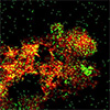
Schematic illustration of DNA-templated assembly of metal sulfide nanoparticles onto 2D MoS₂ surfaces, enabling spatially controlled construction of mixed-dimensional heterostructures with tunable optoelectronic properties. (Image: Reprinted from DOI:10.1002/adfm.202502140, CC BY) (click on image to enlarge)
The researchers began by exfoliating MoS₂ into few-layer flakes suspended in water. These flakes were functionalized with 30-base-long single-stranded DNA that carried a sulfur group at one end to anchor it to the MoS₂ surface. To this DNA scaffold, they then attached shorter complementary DNA strands that had been loaded with metal ions such as lead (Pb²⁺), cadmium (Cd²⁺), or copper (Cu²⁺). These strands directed the formation of metal sulfide nanoparticles at specific sites along the DNA when exposed to a sulfide source. By targeting different segments of the 30-base strand—positions near the MoS₂, in the middle, or further away—they controlled the spacing between each nanoparticle and the 2D surface.
This modular assembly allowed them to construct nanohybrids where the composition and geometry of the system could be precisely tuned. They demonstrated the technique using PbS, CdS, and CuS nanoparticles, either individually or in combination, placed at defined locations along the DNA. Microscopy confirmed that these nanoparticles appeared at the intended distances, and atomic force measurements revealed clear height differences corresponding to the programmed arrangement.
Spectroscopic analysis showed that changing the distance between the nanoparticles and the MoS₂ altered the material’s absorption of light. For hybrids containing PbS and CdS, new absorption features appeared near 710 nanometers, which the researchers attributed to the formation of trions—charged excitonic states consisting of two electrons and one hole. These trions were more prominent when nanoparticles were positioned closer to the MoS₂ surface, suggesting a doping effect induced by proximity. In contrast, CuS/MoS₂ systems showed different spectral features, reflecting the difference in electronic structure and coupling behavior.
The team tested the effect of external voltage on trion intensity and found that applying a positive bias increased the absorption at 710 nanometers, consistent with enhanced electron doping. Raman spectroscopy further supported these findings, showing characteristic shifts in MoS₂ vibrational modes as doping levels changed. The researchers also observed that the DNA itself contributed to electronic modulation. The phosphate backbone of the DNA introduced slight n-type doping even before nanoparticle attachment, which was then modified as nanoparticles formed.
To assess how this tunable doping and absorption translated into device performance, the team constructed phototransistors using monolayer MoS₂ field-effect transistors. After functionalizing these devices with DNA-templated PbS or CuS nanoparticles, they measured photocurrent responses under different wavelengths of light. Devices with PbS placed near the MoS₂ showed strong photocurrent enhancement at 650 and 700 nanometers, consistent with the observed trion-related absorption features.
Quantitative analysis revealed that these devices reached detectivities of up to 2.4 × 10¹⁵ Jones, among the highest reported for such systems. Detectivity is a measure of a photodetector’s ability to detect weak signals over noise, and values in this range are suitable for sensitive imaging and sensing applications. Responsivity, which quantifies how much current is generated per unit of incident light, also reached values as high as 3 × 10⁴ A/W. These figures are competitive with other nanohybrid photodetectors based on van der Waals interfaces but were achieved here through a fully aqueous, DNA-based method.
Notably, the researchers extended their approach to create heterostructures containing multiple types of nanoparticles on a single DNA strand. In one configuration, PbS and CuS nanoparticles were grown on adjacent segments of the DNA, enabling a phototransistor that responded to both 700 and 808 nanometer light. This spectral tuning is important for devices that operate across the visible and near-infrared ranges, such as telecommunications sensors, biomedical imaging systems, and environmental monitors.
The devices maintained fast response times on the order of half a second. At 808 nanometers, the dual-nanoparticle devices reached responsivity values as high as 3.5 × 10⁴ A/W and detectivity up to 3.3 × 10¹⁵ Jones—figures that match or exceed the best-performing MoS₂-based photodetectors reported to date. The ability to design specific wavelength responses through nanoparticle composition and positioning is a feature not easily achieved through conventional fabrication.
The key innovation in this work lies in the use of DNA as a precise, programmable scaffold for constructing functional nanomaterials with tunable electronic and optical properties. The strategy avoids damage to the 2D substrate, allows for multiple types of nanoparticles in a single structure, and is compatible with solution-based processing. It also opens the door to broader application of biomolecular assembly in materials science.
The work demonstrates how biochemical tools can be repurposed for electronic design, enabling a new level of spatial control that traditional physical assembly techniques cannot easily match. By using DNA to modulate both structure and function, the researchers have shown a way to systematically explore and engineer the interactions between nanoscale components in a controlled environment.
This platform could be extended beyond MoS₂ to other 2D semiconductors, or adapted to introduce catalytic or sensing functionality via different nanoparticle types. As the demands for miniaturized, multi-functional, and wavelength-specific devices grow, strategies like this—combining biological precision with electronic function—are likely to play an increasingly central role in materials development.
Get our Nanotechnology Spotlight updates to your inbox!
Thank you!
You have successfully joined our subscriber list.
Become a Spotlight guest author! Join our large and growing group of guest contributors. Have you just published a scientific paper or have other exciting developments to share with the nanotechnology community? Here is how to publish on nanowerk.com.