A pulsed thermal shock technique produces micron-thick flexible graphite films ten times faster than conventional methods without sacrificing crystalline quality or thermal performance.
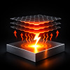
(Nanowerk Spotlight) Crystalline graphite conducts heat along its planes faster than any metal, and when thinned to just a few micrometers it becomes flexible enough to line the inside of a foldable phone or wrap around a medical sensor. That rare pairing of thermal performance and mechanical compliance has made micron-thick graphite films one of the most sought-after materials in advanced electronics, with uses ranging from flexible thermal spreaders and electrothermal actuators to EUV lithography shielding and conformal electronic skins.
Graphite’s layered structure, in which carbon sheets are held together by weak interlayer forces, has also proved essential in fundamental physics, enabling discoveries in band structure engineering and quantum Hall effect research. But the manufacturing has not kept pace with the demand: producing graphite with the necessary structural order still requires days of processing at temperatures above 2500 °C, a constraint that has kept high-quality flexible graphite confined to small-batch laboratory settings.
The standard benchmark, highly oriented pyrolytic graphite (HOPG), grows at roughly 0.1 μm per hour under sustained temperatures of 2500 to 3000 °C and pressures of 30 MPa, with production cycles exceeding 24 hours. Kish graphite, crystallized from molten iron-carbon mixtures, forms only micron-sized grains with porosity above 30% and iron contamination in the hundreds of parts per million, requiring further annealing at 2000 °C. Converting polymer films into graphite demands similarly extreme conditions, with days at 3000 °C needed to produce material that still struggles with crystallinity below 10 μm thickness.
A lower-temperature alternative uses nickel or cobalt foils as both catalyst and template: carbon dissolves into the hot metal and then separates out as graphite layers during cooling. But carbon diffuses slowly under steady-state conditions, capping film thickness at the submicron range unless processing stretches over days.
A study now published in Nature Communications (“Rapid synthesis of micron-thick flexible graphite films via non-equilibrium carbon flux engineering”) takes a fundamentally different approach by pushing carbon transport far from thermodynamic equilibrium. The method, called pulsed Joule heating-induced carburization (PJHIC), delivers rapid electrical pulses to polymer-coated nickel foils, generating thermal shocks that drive carbon dissolution and segregation at rates more than ten times faster than any previously reported technique.
Schematic of pulsed Joule heating-induced carburization strategy and rapid growth characterization. (Image: Reproduced from DOI:10.1038/s41467-026-70028-8, CC BY ) (click on image to enlarge)
The process starts with a thin layer of polymethyl methacrylate (PMMA) spin-coated onto a 50 μm-thick nickel foil inside a sealed chamber filled with argon. Pulsed current through graphite electrodes heats the foil to 1300 °C at rates above 300 °C per second. This thermal shock breaks apart the polymer, releasing carbon atoms that dissolve into the nickel.
After a brief hold at peak temperature, controlled water cooling at about 70 °C per second triggers forced segregation. As the metal cools, its capacity to hold dissolved carbon drops sharply, and the excess carbon crystallizes on the surface as ordered graphite.
The speed of this process stems from the thermodynamic pressure created by rapid cooling. Dropping from 1300 °C to 1000 °C in four to five seconds produces a carbon excess of about 0.28 wt% in the nickel, lowering the energy barrier for graphite nucleation so substantially that new crystals form rapidly and densely across the surface. The resulting carbon flux reaches approximately 2.1 × 10²² atoms per square meter per second, about a hundred times higher than state-of-the-art chemical vapor deposition.
Crucially, the work reveals that carbon species travel through the bulk metal at rates exceeding 4.5 μm per second under these non-equilibrium conditions, providing new insight into how rapidly carbon can move through a solid when conventional diffusion limits are bypassed.
Depth profiling with time-of-flight secondary ion mass spectrometry, a technique that maps elemental composition layer by layer, tracked carbon’s distribution through the nickel at different stages. After 10 seconds, carbon appeared uniformly throughout the metal bulk, indicating dissolution before any surface precipitation. By 12 seconds, a distinct graphite layer had formed, pinpointing the onset of segregation within a narrow two-second window.
At 72 seconds, continuous films roughly 800 nm thick covered the surface. Three-dimensional mapping revealed that graphite grew preferentially along nickel grain boundaries, where looser atomic packing creates faster diffusion pathways. With a growth duration of 61 seconds, the maximum vertical growth rate reached 730 nm per minute. Because segregation occurs predominantly during the brief cooling phase, the instantaneous rate reaches approximately 12,000 nm per minute.
A single thermal cycle can only segregate about 800 nm of graphite, limited by how much carbon the nickel can dissolve at once. To push beyond this ceiling, the team developed a cyclic protocol: repeated rounds of 120 seconds of heating followed by 30 seconds of forced cooling. Each cycle dissolves additional carbon and deposits another layer. Film thickness scaled linearly with cycle number, reaching 1 to 5 μm over 1 to 50 cycles on both nickel and cobalt foils. A 5 μm-thick film required roughly two hours. The resulting films are continuous, crack-free, and structurally uniform across centimeter-scale areas.
Characterization confirmed that the speed did not come at the expense of order. Raman spectroscopy showed minimal defect signals across more than 10,000 measurement points. X-ray diffraction measured an interlayer spacing of 3.355 Å, virtually identical to HOPG, natural graphite, and Kish graphite. Electron microscopy confirmed ABA (Bernal) stacking at the atomic scale. Crystal domain mapping revealed in-plane grain sizes exceeding 1.2 mm, far larger than the 100 to 200 μm grains of the underlying nickel, indicating that graphite layers propagated across substrate grain boundaries rather than being confined by them.
Thermal conductivity, measured by time-domain thermoreflectance, reached 1314 W m⁻¹ K⁻¹ along the plane and 7.51 W m⁻¹ K⁻¹ through the thickness. These values closely match Kish graphite and approach HOPG, while substantially surpassing natural graphite at 904 W m⁻¹ K⁻¹.
The non-equilibrium process does introduce grain boundaries, point defects, and surface wrinkles, leaving the films short of single-crystal perfection. But the method has already scaled to 12 cm × 5 cm on both nickel and cobalt substrates, and the researchers note that further optimization of segregation kinetics could narrow the gap between speed and structural quality.
The underlying principle, using large thermodynamic driving forces from rapid thermal cycling to accelerate atomic transport in solids, extends beyond graphite. The researchers propose that non-equilibrium carbon flux engineering could serve as a general strategy for the high-throughput synthesis of other functional layered materials requiring both atomic-scale precision and industrial-scale viability.
For authors and communications departmentsclick to open
Lay summary
Prefilled posts
Nanowerk Newsletter
Get our Nanotechnology Spotlight updates to your inbox!
Thank you!
You have successfully joined our subscriber list.
Become a Spotlight guest author! Join our large and growing group of guest contributors. Have you just published a scientific paper or have other exciting developments to share with the nanotechnology community? Here is how to publish on nanowerk.com.