A silver single-atom chain demonstrates atomic-scale strain sensing and piezoresistive effects, advancing nanotechnology and nanoscale sensing capabilities.
(Nanowerk Spotlight) At the scale of individual atoms, materials behave in ways that defy everyday intuition. Stretch a metal wire by a few micrometers and its resistance changes only slightly. Stretch a chain of just a few atoms by a fraction of a nanometer, and the flow of electrons can change dramatically, shifting a structure from highly conductive to nearly insulating. Yet directly observing how atomic-scale strain transforms electronic transport has remained out of reach. Microscopes could show atoms, and electrical measurements could track currents, but not at the speed and precision needed to capture both at once. The critical link — seeing and measuring how a single atom chain stretches, strains, and conducts in real time — was missing.
Now, researchers at the City University of Hong Kong have bridged that gap. Using an exceptionally stable chain of silver atoms, they have demonstrated that atomic-scale strain sensing is not only possible, but that the resulting changes in resistance are far larger than anything seen at the macroscopic level. By combining direct mechanical manipulation with real-time electrical measurements inside a transmission electron microscope, they have captured a complete, atom-by-atom picture of how strain controls electronic transport at the most fundamental scale.
Their study, published in Advanced Science (“Atomic-Level Strain Sensing and Piezoresistance Effect in a 1D Single-Atom Chain”), focuses on the construction and testing of a one-dimensional silver atom chain, fabricated in situ under a dual spherical aberration-corrected transmission electron microscope. Using a nanomanipulator capable of sub-angstrom precision, the team exfoliated atomically clean surfaces and formed stable atomic chains by bringing two silver crystals into contact under carefully controlled conditions. By applying a low bias voltage, they encouraged silver atoms to diffuse and bond across the interface, forming a suspended chain just one atom wide.
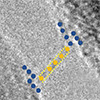
Time-sequence transmission electron microscope images showing the formation and stretching of a silver single-atom chain between two aligned silver nanocrystals under an applied bias voltage. The chain extends up to five atoms in length while maintaining structural integrity during tensile deformation. Atomic positions shift progressively under applied stress, enabling real-time observation of atomic-scale strain effects. The schematic diagram on the right illustrates the in situ experimental setup, where a nanomanipulator positions and tensions the atomic chain between a silver-coated tungsten tip and a semi-copper grid. (click on image to enlarge)
As the atomic chain formed and stretched, the researchers monitored both its atomic structure and electrical conductance. High-resolution imaging captured the positions of individual atoms, allowing for precise calculation of strain as the chain elongated. Simultaneously, they measured the current flowing through the chain, revealing a strong dependence of electrical resistance on strain. Small changes in interatomic distance produced significant, measurable changes in conductance, confirming that the structure behaved as an ultra-sensitive strain sensor at the atomic scale.
The mechanical stability of the chain at room temperature was notable. Over a period of about 30 seconds, the chain endured repeated tension and compression cycles without catastrophic failure. During stretching, the interatomic distances varied nonuniformly along the chain, leading to localized regions of higher and lower strain. These variations affected how electrons moved through the structure. In regions where atoms were pulled further apart, electron scattering increased, reducing conductivity. Where atoms remained closer, conduction pathways remained more robust.
Quantitative analysis showed that the piezoresistance coefficient — the change in resistance per unit strain — was approximately four times larger than that measured in bulk silver wires. The gauge factor, which measures strain sensitivity, reached a value of about 13.5 compared to 3.35 for macroscopic silver. This enhancement is significant because it confirms that atomic-scale structures respond much more sensitively to mechanical deformation, providing a new pathway for precision sensing at nanometer and even atomic scales.
To understand the mechanisms behind the observed piezoresistive effect, the researchers turned to computational modeling. Using a density-functional-based tight-binding method, they simulated the electronic structure of strained silver atom chains connected to bulk electrodes. The simulations focused on how strain altered the projected density of states near the Fermi level — the key region determining electronic conduction.
The calculations revealed that at low strains, the dominant conduction channel formed by s-orbital electrons remained stable. However, as strain increased beyond about 10 percent, changes emerged in the electronic structure. A pseudo-bandgap began to form near the Fermi level, reducing the density of available conduction states. This transition explained the experimentally observed reduction in current with increasing strain. Despite these changes, the simulations confirmed that silver atom chains maintained their mechanical and conductive properties over a wide range of strain values, aligning closely with the experimental results.
This work marks a significant advance because it combines direct mechanical manipulation, real-time electrical measurement, and atomistic modeling to fully characterize piezoresistive behavior at the ultimate limit of material scaling. Unlike macroscopic or even nanoscale structures, where defects, impurities, and thermal effects complicate measurements, the silver atom chain offers a near-ideal system for studying pure strain-induced changes in electronic transport.
Beyond its immediate scientific value, the study points toward practical applications. Conventional TEM imaging struggles to capture fast dynamic events such as atomic rearrangements, defect formation, or phase transitions, due to limited frame rates. Integrating strain sensors based on single-atom chains could allow researchers to monitor such events with much higher temporal resolution. Because the sensing is electrical rather than optical, it avoids the constraints of image acquisition speed and could detect rapid structural changes as they happen.
The concept also opens possibilities for next-generation nanoelectromechanical systems (NEMS). Devices built from or incorporating single-atom or few-atom structures could achieve unprecedented sensitivity and speed, enabling new approaches to nanoscale sensing, mechanical switching, and flexible electronics. Moreover, while silver was the material chosen here for its diffusion characteristics and stability, the same principles could extend to other metals or low-dimensional materials with tunable electronic properties.
By demonstrating that single-atom chains can serve as both structural elements and active sensors, the research broadens the understanding of how mechanical and electronic properties intertwine at the atomic level. It shows that materials can be engineered not just by composition and size, but by the precise arrangement and movement of individual atoms under external forces. As techniques for controlling and observing atomic-scale structures continue to improve, studies like this lay the groundwork for new classes of dynamic, responsive materials operating at the smallest scales possible.
Get our Nanotechnology Spotlight updates to your inbox!
Thank you!
You have successfully joined our subscriber list.
Become a Spotlight guest author! Join our large and growing group of guest contributors. Have you just published a scientific paper or have other exciting developments to share with the nanotechnology community? Here is how to publish on nanowerk.com.