| Jun 02, 2026 |
A vacuum channel transistor controls electrons at the cathode to suppress gate leakage, letting it work inside amplifiers and NAND and NOR logic gates.
(Nanowerk News) A research team in China has built a vacuum channel transistor that works inside functional integrated circuits, clearing a flaw that kept the technology out of working circuits for more than a decade. The device sends electrons through a vacuum or air gap instead of through silicon, and its design suppresses the stray gate current that ruined earlier versions.
|
|
Researchers at Shanghai Jiao Tong University and Shaoxing University report the work in the journal Microsystems & Nanoengineering (“Research on unit circuits based on cathode modulated vacuum/air channel electron tube”).
|
Key Findings
- The device suppresses gate leakage current below 10⁻¹¹ A by controlling the electron supply inside the cathode rather than steering electrons toward the anode.
- It is the first vacuum or air-channel electron tube to run inside functional integrated circuit blocks, including amplifiers and NAND and NOR logic gates.
- It is made with standard chip fabrication processes on silicon-on-insulator wafers and works at room temperature in ordinary air.
|
|
Engineers have studied planar vacuum electron tubes, a class sometimes called vacuum channel transistors, as a possible replacement for the silicon transistor. The appeal is speed. Electrons crossing a vacuum can move close to the speed of light, roughly a thousand times faster than electrons forced through silicon. That gap promised circuits far quicker than any built from conventional transistors, which is why the idea has drawn steady interest.
|
 |
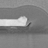
| a The band schematic diagram of the device’s working principle. b Schematic of the CMVET device section. c Chip photo. d Device symbol. e SEM diagram of the device. (Image: Reproduced from DOI:10.1038/s41378-026-01234-z, CC BY) (click on image to enlarge)
|
|
A single problem defeated every earlier design. To control the current, the tube relies on a gate, but as the gate did its job, many electrons struck it instead of reaching the anode, the electrode meant to collect them. The result was a steady leak of current through the gate. That leakage made it impossible to wire the tubes into real circuits, and the field stayed stuck.
|
|
The new device, a cathode-modulated vacuum/air-channel electron tube, or CMVET, fixes the leak by reversing the gate’s role. Earlier tubes used the gate to block or redirect electrons already heading for the anode. This design instead uses the gate to change how many electrons are available inside the cathode, the electrode that releases them. With the gate managing supply rather than catching electrons in flight, almost none are lost.
|
|
A back gate sits below the cathode, separated from it by a thin oxide layer. Voltage on this gate bends the energy levels of an extremely thin silicon cathode, just 45 nanometers thick. A positive voltage pulls electrons toward the cathode surface and raises the field-emission current, the flow of electrons drawn off a surface by a strong electric field. A negative voltage pushes them back and lowers it.
|
|
Because every electron leaving the cathode reaches the anode, the gate current falls below 10⁻¹¹ A, far lower than most tubes reported before. The device operates at room temperature and ordinary air pressure. Its electrical behavior also breaks from that of a standard transistor in one important way.
|
|
The output current does not level off as the anode voltage rises. A MOSFET, or metal-oxide-semiconductor field-effect transistor, the type that fills today’s chips, behaves the opposite way, with its current flattening out at higher voltage. The CMVET’s keeps climbing, a property the team calls non-saturating, and it forced the researchers to rethink parts of the circuit design.
|
|
They ran the tube as a common-source amplifier, a differential amplifier, and a cascade amplifier, and as NAND and NOR logic gates. Amplifier gain reached as high as 1.6. The NAND gate switched between about 4.5 and 1.9 volts, the NOR gate between about 4 and 1.1 volts. NAND and NOR are basic building blocks that carry out simple logic decisions inside digital chips.
|
|
Scanning electron microscope images and electrical measurements confirmed the structure and performance. The on-off current ratio came in at roughly 10⁴, and the transconductance at about 23 microsiemens. Transconductance measures how strongly a small change in gate voltage shifts the output current, so a higher figure points to tighter control over the device.
|
|
The authors described why earlier efforts failed and how their approach differs. “We’ve worked on this problem for years, because everyone knows that if you could make vacuum tubes work again at the chip scale, the speed advantage would be enormous,” the authors said. “The reason previous attempts failed was always the same – the gate leaked. By controlling the electron supply at the cathode instead of trying to catch electrons in mid‑air, we finally got rid of that leakage. Seeing the same device work as an amplifier, a differential pair, and even a NAND gate on the test bench was the moment we realized this approach actually has a future.”
|
|
The result points toward monolithic integrated circuits built entirely from vacuum tubes, which could run far faster than today’s transistors. The biggest gains are likely in high-frequency electronics and in harsh settings where solid-state devices struggle. Vacuum and air channels are immune to radiation and keep working across a wide temperature range, so the team suggests uses in satellites, aerospace systems, and defense electronics.
|
|
The fabrication route already fits standard chip production, relying on familiar steps such as deposition, etching, oxidation, and ion implantation. Because these processes are standard across the semiconductor industry, the device needs no separate or unusual manufacturing approach.
|
|
One limitation still stands. Because the output current never settles, gain is capped in some circuit layouts, and the team flags reducing this non-saturating effect as its next engineering target. Even so, by suppressing the gate current at its source, the design clears the barrier that kept vacuum electronics out of functional chips, using fabrication the industry already runs. The path from a single device to a working vacuum-tube logic gate has now been demonstrated.
|