| May 01, 2026 |
A new moire quantum well built from twisted boron nitride layers emits deep-ultraviolet light 20 times more efficiently than aluminum gallium nitride semiconductors.
(Nanowerk News) A research team in South Korea has built a deep-ultraviolet semiconductor that emits light roughly 20 times more efficiently than the materials currently used in UV LEDs. The advance comes from a new quantum structure formed by stacking boron nitride layers at a twist angle, and it targets a wavelength band that conventional semiconductors handle poorly (Science, “Highly efficient, deep-ultraviolet luminescence in hBN moiré quantum wells”).
|
Key Findings
- Twisted boron nitride layers form a new quantum structure the team calls a moiré quantum well.
- The structure emits deep-ultraviolet light roughly 20 times more efficiently than aluminum gallium nitride.
- The 200 to 230 nanometer band it targets can disinfect air and surfaces without penetrating human skin.
|
|
Semiconductor light sources have shaped modern lighting, displays, and lasers across the visible spectrum. Attention has since shifted to ultraviolet wavelengths, which carry shorter wavelengths and higher energy than visible light. Demand for deep-ultraviolet sources, which can inactivate bacteria and viruses, climbed sharply during the COVID-19 pandemic and has remained a research priority.
|
|
Most existing UV LEDs rely on gallium nitride. Replacing some of the gallium with aluminum to form aluminum gallium nitride shifts the emission deeper into the UV. Below 240 nanometers, however, the efficiency of these devices collapses to under one percent, leaving the 200 to 240 nanometer window largely inaccessible to commercial technology.
|
|
The POSTECH team set aside gallium nitride entirely and turned to boron nitride, a van der Waals semiconductor in which atoms are tightly bonded within each atomic layer but only loosely held to neighboring layers. Because the interlayer bonding is weak, individual layers can be peeled apart and restacked at chosen angles, a freedom that conventional crystals do not offer.
|
 |
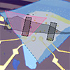
| Electroluminescence from a moiré quantum well device built with twisted boron nitride layers. The optical micrograph (top left) shows the device structure, with graphene electrodes contacting boron nitride flakes, while the spatial map (bottom left) reveals localized light emission in the 200 to 230 nanometer range. Emission spectra (right) compare H-type and R-type stacking configurations against an AA’-stacked bulk reference, with the twisted structures producing far stronger deep-ultraviolet output across a range of injection currents. (Image: POSTECH)
|
|
When the researchers rotated boron nitride layers relative to one another and stacked them, the rotation produced a moiré pattern that gave rise to a new quantum-well structure. They named it a moiré quantum well. It traps electrons within a nanometer-scale region, a level of confinement well suited to producing short-wavelength photons.
|
|
Professor Jonghwan Kim described the conceptual shift involved. He said, “This is a conceptual shift that extends the unique moiré quantum physics observed in van der Waals materials from two-dimensional systems to three-dimensional materials,” adding, “This research will serve as a starting point for designing new quantum materials and developing next-generation optoelectronic devices.”
|
|
Quantum effects in van der Waals materials have mostly been studied in atomically thin films such as graphene. The new work shifts that picture by showing a distinctive two-dimensional quantum-well structure can be produced from a three-dimensional boron nitride crystal through stacking and rotation alone.
|
|
Wavelength matters for human safety as well as engineering. Commercial deep-UV disinfection currently relies on the 260 nanometer band, which damages skin and eyes on direct exposure and therefore cannot be used continuously around people. Light in the 200 to 230 nanometer band is considered relatively safe because it does not penetrate the stratum corneum, the outermost layer of skin.
|
|
A practical light source in that safer band could support continuous disinfection of air and surfaces in hospitals, schools, and public transportation, where high foot traffic raises the risk of pathogen transmission. The POSTECH approach removes a key barrier to building such devices by producing usable emission efficiency in a window where conventional semiconductors fail.
|
|
Hyuk Chae Koo, First Vice Minister of the Ministry of Science and ICT, framed the result as evidence of sustained investment. He stated, “Professor Jonghwan Kim is a researcher who has steadily pursued long-term research in a single field over the past decade through MSIT’s basic research program,” adding, “We will continue to provide full support to create an environment where researchers can immerse themselves in long-term research without being overly pressured by short-term outcomes.”
|
|
The team plans to extend the work toward functional deep-UV light-source devices and to explore broader uses of the moiré quantum well concept in quantum photonic technologies.
|