Twisting atomically thin hybrid perovskite crystals against other 2D materials at controlled angles tunes interlayer coupling and device performance, extending twist-angle engineering to soft optoelectronics.
(Nanowerk Spotlight) Rotating one atomically thin crystal against another by just a few degrees can transform the electronic properties of the stack. This insight underpins the field of twistronics, which has reshaped condensed matter physics over the past several years, producing superconductivity in twisted bilayer graphene and enabling fine control over excitons in transition-metal dichalcogenide pairs. But the materials that respond so cleanly to rotational tuning share a common trait: they are rigid, purely inorganic sheets with stiff lattice frameworks.
Halide perovskites present a different structural challenge. Their crystal lattices are soft and deformable, bulky organic molecules sit wedged between inorganic sheets, and strong electron-phonon coupling dominates their optical behavior. Early explorations suggested that perovskite-based heterostructures could host twist-dependent phenomena, but no study had systematically mapped how rotation translates into device-level performance gains across a controlled angular series.
A study published in Advanced Energy Materials (“Twist‐Angle Engineering of Atomically Thin Halide Perovskite/WSe₂ Van der Waals Heterojunctions for Enhanced Optoelectronic Performance”) provides that map. The research team fabricated atomically thin heterojunctions pairing the layered perovskite (PEA)₂PbBr₄ with monolayer WSe₂ at six defined twist angles from 0° to 15°. Increasing the twist strengthened interlayer coupling at every level measured and improved all device figures of merit, culminating in a 15° heterojunction with a photoresponsivity of 2.8 A W⁻¹ under 405 nm illumination.
The two materials bring different assets to the stack. (PEA)₂PbBr₄ absorbs light strongly and produces intense excitonic emission even as a bilayer. WSe₂ offers high carrier mobility and gate-tunable transport. Stacking them creates a type-II band alignment: the energy levels offset so that electrons collect in one layer and holes in the other. This built-in charge separation forms the basis for efficient photodetection.
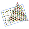
Schematic diagram and structural characterization of (PEA)2PbBr4/WSe2 heterojunction construction. (a) (PEA)2PbBr4/WSe2 heterojunction construction process diagram. (b) Schematic diagram of atomic model of heterojunction. The white triangle is a schematic diagram of the WSe2 atomic model, and the blue quadrilateral is a schematic diagram of the (PEA)2PbBr4 atomic model. (c-h) Bright field optical microscopy (BF-OM) at 0°, 5°, 7°, 10°, 12° and 15° twist angles. The white lines indicate the angle between the (PEA)2PbBr4, and the WSe2. Scale bars: 20 µm. (i) SEM images of heterojunctions, with white triangular wireframes representing WSe2 and blue quadrilateral wireframes representing (PEA)2PbBr4. (Image: Reproduced with permission from Wiley-VCH Verlag)
The team grew triangular monolayer WSe₂ on silicon substrates by chemical vapor deposition, prepared rectangular perovskite crystals separately, then exfoliated and transferred the perovskite onto WSe₂ at controlled orientations. Atomic force microscopy confirmed the expected layer thicknesses. With the heterostructures assembled, the next step was establishing whether the twist angle actually controls interlayer interaction.
As the twist increased from 0° to 15°, characteristic lattice vibration modes in both materials shifted to higher frequencies. This phonon hardening signals that restoring forces on atoms near the interface grow stronger with rotation, a direct marker of tighter coupling driven by interfacial charge redistribution and subtle strain.
Photoluminescence measurements told a consistent story. Emission peaks from both the perovskite and WSe₂ shifted to longer wavelengths across the twist series, while their intensity dropped. Stronger hybridization narrows the effective bandgaps of both layers, and efficient spatial separation of electrons and holes suppresses radiative recombination. Both effects grew monotonically with twist angle, confirming that rotation acts as a continuous dial for coupling strength.
Density functional theory calculations supplied a microscopic framework. Across all six angles, the heterostructure maintained an indirect bandgap with type-II character, the valence band maximum sitting on the perovskite and the conduction band minimum on WSe₂. The calculated bandgap narrowed steadily from 0° to 15°, reflecting enhanced orbital hybridization that pushes band edges closer together and increases the density of states available for carrier transport.
These spectroscopic and computational trends carried through to device performance. All six heterostructures produced diode-like current-voltage behavior, consistent with a built-in electric field from the type-II offset. Even at 0° twist, forming the heterojunction boosted current roughly 230-fold over bare WSe₂. The turn-on voltage dropped monotonically with increasing twist, matching the predicted bandgap narrowing.
Under 405 nm illumination, the 15° device achieved a photoresponsivity of 2.8 A W⁻¹, an on/off ratio of 2.33 × 10⁵, and a hole mobility of 117.1 cm² V⁻¹ s⁻¹. Under 532 nm light, the photoresponsivity exceeded that of bare WSe₂ by a factor of about 244. These values compare favorably with previously reported perovskite and transition-metal dichalcogenide heterostructure photodetectors under similar conditions.
Reproducibility data strengthen the case that twist angle is the controlling variable. Three independent devices at each angle showed consistent electrical behavior, and repeated photoluminescence measurements yielded negligible deviations in peak position. Control experiments confirmed that the diode-like rectification originates from the heterointerface, not from electrode reactions.
The broader significance lies in extending twist-angle engineering beyond rigid inorganic stacks into a hybrid organic-inorganic material system. The soft lattices and strong electron-phonon coupling of layered perovskites could easily have weakened the twist-dependent trends seen in graphene and dichalcogenide bilayers. Instead, the rotational response proved clean and monotonic. The interlayer orientation rather than the chemical formula serves as the primary lever for optimization, offering a composition-agnostic strategy for designing ultrathin optoelectronic devices.
For authors and communications departmentsclick to open
Lay summary
Prefilled posts
Nanowerk Newsletter
Get our Nanotechnology Spotlight updates to your inbox!
Thank you!
You have successfully joined our subscriber list.
Become a Spotlight guest author! Join our large and growing group of guest contributors. Have you just published a scientific paper or have other exciting developments to share with the nanotechnology community? Here is how to publish on nanowerk.com.