A thin diamond film encapsulates gold nanoparticles into a reusable SERS substrate that survives acid, abrasion, and months of storage without losing sensitivity.
(Nanowerk Spotlight) Every molecule scatters light in a slightly different way, and Raman spectroscopy reads those differences like a chemical barcode. The technique is powerful but inefficient: only about one in ten million photons undergoes the energy shift that carries useful information. That weakness matters little when analyte is abundant, but it makes detecting trace or low-concentration compounds impractical without amplification.
SERS, or surface-enhanced Raman spectroscopy, provides that amplification by placing molecules near metallic nanoparticles that concentrate incident light into intense electromagnetic fields, boosting the signal by thousandfold or more.
Yet the gold nanoparticles and silver nanoparticles responsible for that amplification are remarkably fragile. Physical contact and even vibration can destroy them. They sit atop paper or silicon substrates, attached only by weak van der Waals forces, and most are discarded after a single measurement. Samples must be brought to the instrument rather than the instrument taken to the sample.
The obvious fix — shielding the nanoparticles behind a protective layer — runs into a fundamental constraint. SERS enhancement decays sharply with distance. Any coating thick enough to offer real protection risks blocking the electromagnetic fields it is meant to preserve. Thin oxide films and metal shell architectures have improved chemical resistance or thermal stability in isolation, but none has delivered the mechanical hardness, chemical inertness, and optical transparency needed for a reusable substrate that survives harsh conditions.
Diamond offers all three. It resists most chemicals, ranks among the hardest known materials, and transmits light across a broad spectral range. A study published in Advanced Functional Materials (“Through Diamond Robust Surface Enhanced Raman Spectroscopy”) now demonstrates that a thin diamond film can protect SERS nanoparticles without suppressing their performance.
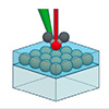
Illustration of SERS measurement protocols. (a) Standard exposed NP SERS measurement “front-illumination” configuration on a paper substrate. (b) Diamond SERS measurement “front-illumination” configuration. NPs are protected against the target environment by a thin polycrystalline diamond (PCD) film grown around metallic NPs on a single crystalline diamond (SCD) substrate. (c) Through diamond SERS measurement “rear-illumination” configuration. Where the target environment is to the “front” of the substrate and spectrometer setup protected a the substrate “rear”. (d) Illustration depicting potential envisioned real-world application of diamond SERS using “rear-illumination” configuration. (e) Standard SERS measurement protocol whereby substrates are single use and fragile. (f) Diamond SERS measurement protocol where substrate ability to resist damage from any analyte removal cleaning suggests a near-infinite reusability. (Image: Reproduced from DOI:10.1002/adfm.202525656, CC BY) (click on image to enlarge)
The research team grew a polycrystalline diamond layer around gold nanoparticles on a single-crystal diamond substrate, then etched it back to a precise thickness at which protection and plasmonic enhancement coexist. The encapsulated substrate matched the enhancement of commercial SERS devices and survived acid baths, solvent sonication, sandpaper abrasion, and six months of open storage without any loss of signal.
Illuminating through the diamond from behind also produced stronger enhancement than conventional front illumination, opening a path toward sealed sensing devices in which all optics sit safely behind the diamond window.
The central question the team faced was whether nanoparticles buried inside diamond could still amplify signals from molecules on the outer surface. Gold nanoparticles were produced on a single-crystal diamond substrate by depositing a thin gold film and heating it in a hydrogen plasma. Surface tension broke the continuous film into discrete particles ranging from 2 to 50 nm in diameter. A polycrystalline diamond layer grown over them by chemical vapor deposition sealed the particles beneath approximately 104 nm of material.
That thickness blocked all Raman enhancement. The team thinned the film incrementally using oxygen plasma etching, creating zones of varying thickness across the substrate. After each step, a gold etchant dissolved any particles that had broken through the surface. This guaranteed that all measured enhancement came exclusively from nanoparticles still sealed within diamond.
The optimal thickness proved to be 31.5 nm. At that depth, the largest nanoparticles sat just nanometers below the diamond surface, close enough for their electromagnetic fields to reach analyte molecules above. The ratio of diamond carbon to non-diamond carbon held steady across the entire film depth, confirming consistent material quality rather than uneven encapsulation.
Using Rhodamine 6G as a probe molecule, the optimized substrate yielded an enhancement factor of 6.2 × 10³ with 532 nm laser excitation, comparable to commercially available SERS substrates. Nanoscale pits left in the diamond surface after exposed nanoparticles were etched away may contribute additional enhancement. Such diamond nanopits have independently been shown to boost SERS signals, suggesting the etching process introduced a secondary amplification mechanism.
Sending the laser through the single-crystal diamond from behind produced 1.8 times stronger enhancement than front illumination. The polycrystalline overgrowth contains more non-diamond carbon and scatters light more than the pristine single crystal beneath it. Rear illumination avoids these losses. This geometry also means a laser and spectrometer can sit sealed behind the diamond window while only the sensing surface contacts the target environment.
The substrate detected Rhodamine 6G down to 1 × 10⁻⁶ M, roughly one part per million, matching commercial sensitivity. Durability testing then pushed the platform beyond what any previous SERS substrate has survived. The researchers subjected it to gold etchant, hot acid cleaning, ultrasonic agitation in organic solvents, six months of unprotected storage, and 100 passes of abrasion with fine sandpaper. After every treatment, the Raman signal intensity remained statistically unchanged.
No previous SERS substrate has demonstrated simultaneous resistance to chemical, thermal, and mechanical stress while maintaining stable enhancement over months of storage. The rear-illumination geometry adds a device-level advantage, enabling architectures where sensitive electronics remain protected while the diamond surface faces marine, industrial, or geological environments directly.
A molecular sensor that survives its working conditions and returns the same signal measurement after measurement removes a basic barrier that has kept SERS confined to the laboratory bench.
For authors and communications departmentsclick to open
Lay summary
Prefilled posts
ORCID information
Kieran N. Twaddle (University College London)
, 0009-0009-6680-8452 corresponding author, first author
Richard B. Jackman (University College London)
, 0000-0002-1930-478X corresponding author
Nanowerk Newsletter
Get our Nanotechnology Spotlight updates to your inbox!
Thank you!
You have successfully joined our subscriber list.
Become a Spotlight guest author! Join our large and growing group of guest contributors. Have you just published a scientific paper or have other exciting developments to share with the nanotechnology community? Here is how to publish on nanowerk.com.