A single flat metalens now handles both excitation and fluorescence collection for diamond quantum sensors, enabling nanoscale sensing in spaces too tight for conventional optics.
(Nanowerk Spotlight) Nitrogen vacancy centers are atomic-scale flaws in the diamond crystal lattice, spots where a nitrogen atom sits next to a missing carbon atom. These defects can detect magnetic fields, temperature, and mechanical stress with nanoscale spatial resolution. The mechanism is simple: a green laser makes them glow red, and the brightness of that glow changes with the local environment. Changes in brightness translate directly into quantitative readings of field strength, temperature, or stress.
Researchers have already used this principle to image magnetic textures in materials, map electric currents through graphene, and detect chemical signals inside living cells. The defect itself is atomic in scale, small enough to probe the tightest spaces in physics and biology. But the optics needed to operate it are not.
Focusing the laser and gathering enough returning photons demands a microscope objective, a thumb-sized stack of glass lenses that dwarfs the atomic sensor it reads out. That mismatch has kept diamond quantum sensors too bulky for the narrow pole gaps of strong electromagnets and the surfaces of biological tissue.
Metalenses, flat films of nanoscale pillars that bend light like shaped glass but measure less than a micrometer thick, offer a natural alternative. The problem is that these pillars focus each wavelength differently. The green excitation laser and the red fluorescence need different optical treatment, and a single metalens designed for one blurs the other. Every previous attempt at a metalens-based diamond sensor still relied on a conventional objective for half the job, leaving the optics only partially miniaturized.
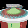
A study published in Advanced Functional Materials (“A Miniaturized Metalens‐Based Spin Defect Quantum Sensor”) reports a single flat metalens that handles both tasks: focusing the 532 nm green laser and collecting the roughly 700 nm red fluorescence, with no conventional objective anywhere in the system. The device is just 1 mm across and thinner than a wavelength of visible light.
Metalens based quantum sensing. (a) Schematic of the experiment. The metalens focuses 532 nm laser to excite NV centers and collects the fluorescence around 700 nm. Microwave(MW) is used to control NV spin state. (b) Simplified energy level of NV center. GS, ground state; ES, excited state; MS, metastable state; PL, photoluminescence. (c) Illustration of excitation laser and NV fluorescence spectrum. (Image: Reproduced with permission from Wiley-VCH Verlag) (click on image to enlarge)
The design splits the metalens into two concentric zones, each tailored to a different wavelength. The inner circle, 474 μm in diameter, focuses the excitation laser. The surrounding ring collects fluorescence. Both zones are built from silicon nitride nanopillars on a quartz substrate. The width of each pillar varies across the surface, bending light at each position by exactly the angle needed for sharp focusing.
The researchers fabricated two versions to test which arrangement works better. In the first, the inner zone handles excitation and the outer ring collects fluorescence. The second reverses the assignment. The reversed layout captured a broader slice of the fluorescence spectrum, about 50 nm versus 30 nm, but the first version produced a tighter laser focus. The team selected the first design for all further experiments.
That choice came at a cost. The metalens collected roughly 16% of the fluorescence that a comparable commercial objective gathers, translating to an estimated 2.5-fold reduction in sensitivity. Its imaging resolution, though, matched conventional optics. Scanning over clusters of nitrogen vacancy centers, the metalens achieved a lateral resolution of 405 nm, hitting the theoretical sharpness limit for its light-gathering power. Axial resolution measured 1.8 μm. Both values agreed closely with simulations.
The team then placed the metalens inside the roughly 3 cm pole gap of an electromagnet, a space far too narrow for a standard objective. Using a diamond plate with implanted nitrogen vacancy centers, they drove coherent spin oscillations with a resonant microwave pulse at 18.6 MHz, confirming that the flat optic supports standard spin control protocols.
Sweeping the microwave frequency at several field strengths produced clean spin resonance spectra up to 4500 G. At that field, the relevant spin transition shifted to 9.65 GHz, a frequency range useful for studying magnetic materials and exploring diamond-based microwave amplifiers.
The researchers next deposited a transparent conducting stripline directly on the diamond surface and drove microwaves through it while scanning beneath the metalens. The resulting maps captured the local field distribution around a bend in the stripline with micrometer-scale detail, matching simulations of current flow in the waveguide geometry.
Achromatic design strategies, such as pillars with more varied cross-sections or stacked metalens layers, could widen the fluorescence bandwidth and close the sensitivity gap. The same architecture could generate specially shaped beams for superresolution imaging, pushing spatial precision below the current optical limit.
Because the approach uses generic flat optics rather than anything specific to diamond, it applies equally to spin defects in other materials such as silicon carbide, hexagonal boron nitride, and gallium nitride. The wavelength-scale thickness and millimeter footprint make this metalens a practical step toward quantum sensors that can operate where conventional microscope optics cannot fit.
For authors and communications departmentsclick to open
Lay summary
Prefilled posts
ORCID information
Xiang-Dong Chen (University of Science and Technology of China)
, 0000-0002-2246-4039 corresponding author
Nanowerk Newsletter
Get our Nanotechnology Spotlight updates to your inbox!
Thank you!
You have successfully joined our subscriber list.
Become a Spotlight guest author! Join our large and growing group of guest contributors. Have you just published a scientific paper or have other exciting developments to share with the nanotechnology community? Here is how to publish on nanowerk.com.