Controlled defects in single-layer graphene pinpoint a critical 20 nm spacing where quantum interference traps electrons and enhances thermoelectric performance at a sharp threshold.
(Nanowerk Spotlight) Electrons do not always behave the way classical physics suggests. In a perfectly ordered crystal, they flow freely, carrying current with minimal resistance. Introduce impurities or structural flaws, and classical intuition says the electrons should slow down, scattering off obstacles but still diffusing through the material. More disorder means more resistance, but transport continues.
Quantum mechanics permits a qualitatively different outcome. Introduce enough randomly placed defects, and electrons do not just slow down. They become spatially confined, trapped in small pockets by the destructive interference of their own wave functions canceling each other out along every possible path forward. Any remaining transport requires electrons to thermally hop from one pocket to the next, a far slower and less efficient process than free diffusion.
The core obstacle is control. Researchers need a material where disorder can be introduced with fine precision across a tunable range. Too little disorder and localization never appears. Too much and the material degrades beyond usefulness. Most bulk disordered systems involve so many competing variables that isolating the localization signal becomes impractical.
Graphene attracted theoretical attention as a candidate platform. Its electrons behave as massless particles, and at low disorder levels, the material’s internal symmetries suppress the backscattering that drives localization. Theory predicts, however, that short-range defects can break those symmetries by forcing electrons to scatter between two inequivalent valleys in graphene’s electronic band structure. This should lift the protection and allow localization to emerge.
Identifying the precise disorder threshold where this transition occurs, and connecting it to measurable transport properties, remained an unresolved experimental challenge.
A study published in ACS Nano (“Quantum Interference and Localization in Disordered Graphene”) provides what its authors describe as the most direct experimental evidence to date for Anderson localization in single-layer graphene. The work also demonstrates that this quantum interference effect enhances thermoelectric performance at a sharply defined disorder threshold.
The research team, based primarily at Clemson University and the College of Charleston, used argon-ion irradiation to introduce defects into single-layer graphene grown by chemical vapor deposition. By varying irradiation power and exposure time, they produced samples spanning a wide range of disorder levels.
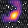
Tight-binding simulations revealing the transition from delocalized electronic states in pristine graphene to strongly confined, spatially localized wave functions as defect concentration increases. (Image: Reproduced with permission from American Chemical Society) (click on image to enlarge)
They quantified that disorder using Raman spectroscopy, a technique that measures how light scatters off a material’s vibrational modes. The ratio of two specific Raman peaks, the disorder-induced D-band and the intrinsic graphitic G-band (I_D/I_G), provided a fingerprint of the average spacing between defects, known as the interdefect distance L_D. Across all samples, L_D ranged from roughly 10 nm to 60 nm.
The central finding is a critical threshold at L_D* ≈ 20 nm, corresponding to I_D/I_G ≈ 0.4, where multiple independent measurements converge to signal the onset of localization.
“At low disorder, electrons in graphene behave as highly mobile, delocalized Dirac fermions,” said Ramakrishna Podila, professor of physics at Clemson University and principal investigator of the study. “What we discovered is a very sharp threshold where quantum interference takes over. Once the defect spacing reaches about 20 nanometers, transport fundamentally changes character with electrons becoming spatially localized, and classical diffusion breaks down.”
Using ultrafast pump-probe reflectivity, the team fired 50-femtosecond laser pulses at the graphene and tracked how quickly excited electrons relaxed back to equilibrium. Both the fast relaxation component τ₁ (driven mainly by electron-electron interactions) and the slow component τ₂ (involving electron-phonon coupling and defect-assisted processes) peaked sharply near L_D* ≈ 20 nm, then declined on either side.
This peak marks a regime where hopping between localized states becomes the dominant relaxation pathway, slowing the return to equilibrium. Below the threshold, electrons sit confined in spatial pockets and must thermally hop between them. Above it, they move diffusively and scatter primarily off lattice vibrations.
Temperature-dependent measurements supported this interpretation. The nonmonotonic peak in relaxation times persisted down to 173 K but flattened and disappeared at 123 K, consistent with the freezing out of thermally activated hopping.
Tight-binding simulations using the kwant quantum transport package provided theoretical confirmation. By progressively removing atoms from a model graphene lattice, the researchers computed the spatial distribution of the ground-state wave function. In pristine graphene, charge probability spread symmetrically across the flake. Once defect density exceeded roughly 1%, the wave function collapsed into isolated high-probability lobes surrounded by near-zero charge density, the spatial signature of localization.
These simulations confirmed that the crossover occurs when the Ioffe-Regel criterion is satisfied: the product of the Fermi wavevector k_F and the electronic mean free path l approaches unity (k_F l ≈ 1), the point where semiclassical transport theory breaks down and quantum interference dominates.
Electrical resistivity measurements on a separate set of graphene samples deposited on quartz corroborated the optical findings. Resistivity increased exponentially as L_D dropped below 20 nm, and the temperature dependence shifted from metallic behavior (nearly constant resistivity) to insulating behavior (resistivity decreasing with rising temperature), both characteristic of thermally activated hopping between localized states.
The Seebeck coefficient, which measures the voltage a material generates in response to a temperature difference, rose with decreasing L_D as the material became more resistive. All irradiated samples showed positive Seebeck values, consistent with the hole-dominated (p-type) doping that vacancy defects introduce.
Both the power factor S²/ρ and the thermoelectric figure of merit zT reached pronounced maxima at L_D* ≈ 20 nm across all measured temperatures. This aligns with a 1996 theoretical prediction by Mahan and Sofo, who argued that optimal thermoelectric performance requires a transport distribution function sharply peaked in energy near the chemical potential.
In plain terms, localization suppresses the contribution of charge carriers at unhelpful energies while allowing those at favorable energies to pass through and generate voltage, effectively sharpening the material’s ability to convert heat differences into electrical output.
Near the localization threshold, narrow bands of extended electronic states bounded by mobility edges, the energy boundaries separating localized from delocalized states, act as sharp energy filters. They selectively transmit charge carriers at favorable energies, boosting the Seebeck coefficient without a proportional increase in resistivity.
“We normally think defects degrade performance,” said Shinto M. Francis, lead author of the study and graduate student in physics and astronomy at Clemson. “But here, controlled disorder sharpens the energy dependence of transport. Near the localization threshold, we see enhanced relaxation and increased thermopower because carriers are effectively filtered in energy.”
The researchers note explicitly that absolute zT values remain low because graphene’s thermal conductivity is inherently high and its gapless band structure limits efficiency.
The significance of the work lies not in graphene’s thermoelectric potential but in its transparency as a model system. Graphene’s well-characterized Raman spectrum allows the interdefect distance to be tracked with a precision unavailable in bulk disordered thermoelectric materials like bismuth-doped lead telluride or aluminum-doped zinc oxide, where evidence for localization-enhanced thermopower remains indirect.
By correlating Raman spectroscopy, ultrafast optical dynamics, electrical resistivity, and Seebeck measurements on a single platform, this study establishes the clearest experimental link yet between a quantifiable disorder threshold and the enhancement of thermoelectric properties through Anderson localization in a two-dimensional system.
Graphene may never become a practical thermoelectric material. But the results point toward a broader design principle: rather than treating disorder as something to eliminate, engineers may be able to tune it precisely to control electronic localization and optimize energy conversion in other low-dimensional materials.
For authors and communications departmentsclick to open
Lay summary
Prefilled posts
Nanowerk Newsletter
Get our Nanotechnology Spotlight updates to your inbox!
Thank you!
You have successfully joined our subscriber list.
Become a Spotlight guest author! Join our large and growing group of guest contributors. Have you just published a scientific paper or have other exciting developments to share with the nanotechnology community? Here is how to publish on nanowerk.com.