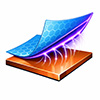
Electrically switchable adhesion in a ferroelectric polymer film enables clean, fast, solvent-free transfer of graphene from copper growth substrates to target surfaces.
(Nanowerk Spotlight) Growing high-quality graphene is no longer the hard part. Chemical vapor deposition can now produce uniform, single-atom-thick carbon sheets at meter scale on copper foils. The hard part is what comes next: peeling that film off its copper birthplace and depositing it, intact and uncontaminated, onto the substrate where it will actually function. This transfer step is where graphene’s journey from laboratory marvel to commercial product consistently stalls.
The standard approach relies on wet transfer: chemical etchants dissolve the copper, and a temporary polymer scaffold ferries the graphene to its destination before organic solvents wash it away. The process works, but it is slow, generates toxic waste, leaves behind polymer residue, and resists scaling to the volumes industry demands.
Dry alternatives, which mechanically peel graphene off copper and press it onto a target, avoid solvents altogether, yet they introduce their own complications. Graphene adheres strongly to the copper on which it grows, with adhesion energies of 0.7–1.5 J m⁻², roughly two to five times greater than the adhesion between graphene and most destination substrates. Peeling under these conditions tears the film or leaves fragments behind.
Previous attempts to improve dry transfer have relied on pre-oxidizing the copper surface with water-based solutions to weaken graphene’s grip, but those steps are slow, dependent on water molecules seeping through defects in the graphene, and difficult to scale. The result is a paradox: a material celebrated for its extraordinary properties remains trapped on the surface where it was made.
A research team based primarily at the National University of Singapore, with collaborators at the École Polytechnique Fédérale de Lausanne and the Institute of Microelectronics of Barcelona, reports a fully dry transfer method that overcomes this adhesion mismatch by exploiting the switchable electric properties of a ferroelectric polymer. Published in (Advanced Materials, “Dry Transfer of CVD Graphene Film Using Adhesion Switchable Ferroelectric Polymers”), the results demonstrate graphene transfers achieving >99% coverage, with lower crack density than either conventional wet or dry methods, on centimeter-scale samples processed in under 5 min by an automated system.
Fully Dry Graphene Transfer with Ferroelectric Supporting Film. a) Schematic illustration of the fully dry transfer process for CVD graphene using a negatively polarized P(VDF-TrFE) film as the mechanical support and transfer layer. b) Molecular structure of P(VDF-TrFE), illustrating its C–F and C–H dipole alignments responsible for its ferroelectric behaviour and polarization direction. c) Schematic of the non-contact Corona poling setup used to induce large-scale polarization in the P(VDF-TrFE) film on the graphene/Cu foil. d) Polarization–electric field (P–E) hysteresis loop for the Au/P(VDF-TrFE)/graphene/Cu capacitor structure after corona poling, demonstrating complete polarization in the P(VDF-TrFE) film. The inset shows the P-E measurement configuration. e) Series of optical microscopy images (150× magnification) of the P(VDF-TrFE)/graphene films transferred onto SiO2/Si substrates, illustrating how graphene delamination coverage and transfer quality depend on the remanent polarization (Pr) state of the P(VDF-TrFE) film. (Image: Reproduced with permission from Wiley-VCH Verlag) (click on image to enlarge)
The method centers on poly(vinylidene-fluoride-trifluoroethylene), abbreviated P(VDF-TrFE), which serves as both the mechanical support layer and the adhesion-control element. Ferroelectric materials possess permanent electric dipoles that can be oriented by an applied electric field and retain that orientation after the field is removed. The team coats a thin film of this polymer onto graphene sitting on copper and then subjects it to a high-voltage, contactless technique called corona poling, which aligns the polymer’s dipoles uniformly. The direction of that alignment determines what happens at the interfaces on either side of the graphene.
Negative corona poling orients the fluorine-rich side of the polymer toward the graphene, inducing p-type doping, meaning it pulls electrons out of the graphene sheet. Density functional theory calculations performed by the team show that this charge redistribution simultaneously weakens the adhesion between graphene and copper (dropping it to 0.29 J m⁻²) while strengthening the bond between the polymer and graphene (raising it to 0.36 J m⁻²). The hierarchy of adhesion flips: the polymer now grips graphene more tightly than copper does, so a mechanical peel lifts the graphene cleanly off the foil.
Positive polarization produces the opposite effect, shifting graphene toward n-type doping and reinforcing its bond to copper, which prevents delamination. Raman spectroscopy, a laser-based technique that probes the vibrational modes of carbon bonds, confirmed these doping effects experimentally. Cantilever beam fracture tests further validated the model: negatively polarized films directed crack propagation along the graphene-copper interface, enabling clean delamination, whereas positively polarized films caused the crack to travel along the polymer-graphene interface instead, leaving graphene adhered to the copper.
Once graphene reaches the target surface, the polymer must release its grip. Here the team exploits another intrinsic property of P(VDF-TrFE): its Curie temperature of approximately 135 °C, above which ferroelectric order vanishes. Heating the stack past this threshold depolarizes the film, neutralizing the electrostatic forces that held it to graphene and restoring only weak van der Waals interactions. A simple adhesive tape then peels the polymer away, leaving behind a graphene surface that atomic force microscopy revealed to be ultrasmooth and virtually free of residue. Raman spectroscopy confirmed that the p-type doping induced during transfer is fully reversible: the final graphene on silicon dioxide sits in a charge-neutral, strain-free state.
The quality gains are concrete. Across 200 optical microscope images spanning four sample batches, the ferroelectric dry-transferred graphene exhibited a crack density of 1 100 μm² per 0.1 mm², compared with 1 600 μm² for conventional wet transfer and 5 800 μm² for thermal-release-tape dry transfer. Almost no cracks larger than 30 μm² appeared. Sheet resistance of the composite polymer/graphene film dropped by 60%, from 667 ± 57 Ω/sq to 270 ± 32 Ω/sq, relative to wet-transferred graphene, while optical transparency across the visible spectrum remained largely unchanged.
The technique extends beyond graphene. The team transferred hexagonal boron nitride films 3–4 nm thick from sapphire to silicon dioxide with preserved crystallinity and surface quality. Monolayer and trilayer molybdenum disulfide likewise survived the process intact. In the case of monolayer MoS₂, the transfer actually reduced surface contamination, suggesting the polymer mechanically strips away loosely adhered particles during delamination.
To move toward practical manufacturing, the team integrated the process into a fully automated batch-to-batch system. The sequence includes slot-die coating of the polymer, corona poling, lamination with thermal release tape, roller-based copper peeling, and hot-press transfer to the target wafer. The copper foils emerged clean, unoxidized, and reusable.
The entire sequence completed in under 5 minutes for centimeter-scale samples. The researchers note the system’s architecture is compatible with roll-to-roll processing at scales up to A3-size sheets, though achieving that will require further engineering of web tension, peel angle, and in-line quality monitoring.
By replacing chemical baths with a reversible electrostatic switch built into the transfer film itself, this method eliminates solvents, etchants, and the contamination they introduce, directly addressing the bottleneck that has separated laboratory-quality graphene from commercial viability.
That the same approach already works for three distinct two-dimensional materials, transferred across different substrate combinations with minimal damage, suggests it could serve as a general-purpose transfer platform as these materials move from prototype to production.
For authors and communications departmentsclick to open
Lay summary
Prefilled posts
ORCID information
Barbaros Özyilmaz (National University of Singapore)
, 0000-0001-7665-4578 corresponding author
Nanowerk Newsletter
Get our Nanotechnology Spotlight updates to your inbox!
Thank you!
You have successfully joined our subscriber list.
Become a Spotlight guest author! Join our large and growing group of guest contributors. Have you just published a scientific paper or have other exciting developments to share with the nanotechnology community? Here is how to publish on nanowerk.com.