| Feb 10, 2026 |
Researchers developed a method to coat curved surfaces with ultra-thin transparent metal films, achieving 88% light transmittance and low resistance like flat electrodes.
(Nanowerk News) From curved displays to smart glasses, many next-generation optoelectronic devices are moving beyond flat surfaces. But one key component has struggled to follow: transparent conducting films. These materials must let light pass through while carrying electrical current, a combination that is already difficult to achieve on flat glass and becomes far more challenging on curved or three-dimensional surfaces.
|
|
Now, researchers at the Harbin Institute of Technology in China report a method for coating complex curved surfaces with ultra-thin (≤10 nm) metal films that are almost invisible to the eye. The work, published in the International Journal of Extreme Manufacturing (“Conformal ultra-thin, ultra-uniform metal films fabricated on non-planar substrates for advanced optoelectronics”), fabricates transparent conductive films with a capping layer show 88% visible transmittance and low sheet resistance of 8.1 Ω·sq-1, offering a practical route to making transparent electrodes that perform as well on curved surfaces as they do on flat ones.
|
 |
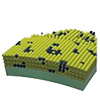
| (a) Schematic illustration of the multi-angle co-velocity trajectory fitting deposition model integrated with the metal co-doping process. Co-doping targets move along the trajectory-coupled path to perform deposition at positions corresponding to different sputtering angles α. (b) Schematic of island morphology in conformal pure ultra-thin metal film. (c) Schematic of continuous morphology in conformal co-doped ultra-thin metal film. (Image: Reproduced from DOI:10.1088/2631-7990/ae3651, CC BY)
|
|
On flat glass or silicon, manufacturers already know how to make transparent conducting films with great precision. But when the surface curves, even slightly, those same techniques tend to fail. The film becomes uneven, growing thicker in some regions and thinner in others. At the nanoscale, such variations can turn a good conductor into a poor one, or make a transparent layer suddenly opaque.
|
|
“Just a few nanometres can make the difference between a working device and a useless one,” says Prof. Heyan Wang, a professor at Harbin Institute of Technology and a lead author of the study.
|
|
To tackle this problem, Prof. Wang and his colleagues took an unconventional approach. Instead of trying to deposit a perfectly uniform layer in a single step, they designed a process that combines several carefully controlled and slightly non-uniform coatings. When these layers are added together, their variations cancel out, producing a film that is uniform overall.
|
|
The method relies on co-sputtering, a common industrial technique in which metal atoms are ejected from solid targets and deposited onto a surface. By precisely controlling the angles, motion paths and speeds involved in the process, the team created what they describe as a multi-angle co-velocity fitting deposition model. The result is a metal film that follows the shape of the surface beneath it, even when that surface curves sharply.
|
|
Using this strategy, the researchers produced silver-based films thinner than 10 nanometres on curved substrates. Despite their extreme thinness, the films remained smooth and continuous rather than breaking into isolated patches, a common problem for ultra-thin metals.
|
|
Tests showed that the curved films transmitted up to 88% of visible light while maintaining very low electrical resistance. These values match those of high-quality transparent conductors made on flat surfaces, something that has been difficult to achieve until now.
|
|
A key part of the success lies in metal co-doping. By introducing small amounts of aluminium during deposition, the researchers stabilized the growth of the silver film. Computer simulations suggest that the added atoms help the metal spread more evenly, allowing it to form a continuous layer instead of clumping into islands.
|
|
The technique is not limited to a single material or shape. The team demonstrated that it can be extended to other metals and to optical dielectric coatings, and adapted to surfaces that are spherical, cylindrical or irregular. They also showed practical examples, including curved transparent electrodes for electromagnetic shielding, decorative coatings that produce colour without pigments, and functional layers for anti-fogging and ultraviolet-blocking eyewear.
|
|
According to Prof. Zhengang Lu, the study’s corresponding author, the work addresses a problem that has quietly constrained the design of future electronics. “As soon as devices stop being flat, many of our most reliable materials stop working as expected,” he says. “This method gives us a way to bring high-performance transparent conductors into three dimensions.”
|
|
Although the experiments were carried out at the laboratory scale, the researchers emphasize that the process is compatible with existing sputtering technologies already used in manufacturing. They are now working to adapt the method for larger areas and more complex shapes.
|
|
As electronic devices increasingly curve to match the world around us and our own bodies, the ability to coat those surfaces with transparent and conductive materials will be essential. This study suggests that, with careful control, even metals just a few atoms thick can be persuaded to bend without breaking.
|


