| Jan 27, 2026 |
Physicists found why holes move slower than electrons in silicon: not defects, but higher intrinsic mass, supporting CMOS-based quantum, cryogenic, and space devices.
(Nanowerk News) UNSW Sydney physicists working with industry partners imec (Belgium) and Diraq (Sydney) have discovered why positive charge carriers called holes move much more slowly in silicon than do electrons, their negative counterparts (Physical Review B, “Holes in silicon are heavier than expected: Transport properties of extremely high mobility electrons and holes in silicon MOSFETs”).
|
|
The finding shows the difference isn’t due to defects or disorder, but because holes are intrinsically heavier than expected. The result suggests that both electron- and hole-based quantum devices, as well as advanced cryogenic and space electronics, could be fabricated using standard CMOS technology, supporting the long-term development of scalable silicon quantum platforms.
|
Understanding the imbalance
|
|
At the ultra-low temperatures required for quantum electronics, silicon transistors behave differently from the ones that power everyday computers. For decades, researchers have observed that electrical current carried by holes moves far more sluggishly than that carried by electrons, even in the cleanest devices.
|
|
A team led by Professor Alex Hamilton at UNSW Sydney has now shown that this sluggish behaviour is not due to impurities or poor fabrication, but to a fundamental feature of silicon’s electronic structure: holes are simply heavier than expected.
|
|
“It was exciting to realise that what looked like a materials problem actually stemmed from the physics of holes and electrons in silicon,” said undergraduate student and lead author Jonathan Wendoloski.
|
Record-setting measurements
|
|
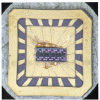
The researchers measured the mobilities of both electrons and holes in silicon transistors known as MOSFETs, using devices fabricated at imec’s 300 mm CMOS foundry and in UNSW’s cleanroom facilities. The results were record-high mobilities: about 40 000 cm²/Vs for electrons and 2 000 cm²/Vs for holes.
|
|
By extending existing theoretical models the team demonstrated that the ten-fold mobility gap arises from the unusual way that energy relates to velocity in silicon, which makes holes seem three times heavier than expected. This heavier effective mass means that holes are more frequently scattered by impurities as they move through silicon, and this slows them down, even in the highest quality devices.
|
|
“It was really nice to see an undergraduate student undertake world-class research with our team, working with industry partners to reach record electron and hole mobilities,” said Prof. Hamilton, senior author on the study.
|
Implications for industry and quantum technology
|
|
By identifying the intrinsic cause of low hole mobility, the study gives device engineers a reliable framework for benchmarking interface quality and guiding future transistor and qubit design. The findings suggest that both electron- and hole-based quantum devices could be fabricated using standard CMOS technology, reducing development risk and accelerating the path to manufacturable, low-temperature electronic platforms. The results also provide key input for engineers developing cryogenic control electronics for quantum, space and sensing technologies.
|
Next steps
|
|
The UNSW team is now extending the same modelling framework to isotopically enriched ²⁸Si devices to confirm the results in qubit-grade material. Further work will explore how these heavy hole properties influence quantum mechanical phenomena such as spin-orbit coupling, as well as the implications for using holes to store and process quantum information in silicon quantum dots.
|
|
These collaborations between UNSW Physics, Diraq, and imec continue to advance Australia’s role in developing scalable, CMOS-compatible quantum hardware and cryogenic technology.
|

