| Jan 27, 2026 |
Researchers show hafnium stannide can host graphene-like electron flow in a robust 3D structure, paving the way for scalable low-energy computing technologies.
(Nanowerk News) University of Liverpool researchers have discovered a way to host some of the most significant properties of graphene in a three‑dimensional (3D) material, potentially removing the hurdles for these properties to be used at scale in green computing.
|
|
Graphene is famous for being incredibly strong, lightweight, and an excellent conductor of electricity and its applications range from electronics to aerospace and medical technologies. However, its two-dimensional (2D) structure makes it mechanically fragile and limits its use in demanding environments and large-scale applications.
|
|
In a paper published in Matter (“Decoupling structural and electronic dimensionality: 2D transport in a 3D honeycomb chiral stacking”), a team of researchers have identified that 3D material, HfSn₂, mimics graphene’s fast, 2D electron flow. This ground-breaking discovery offers opportunities for designing materials that are more stable yet that still show advanced low‑energy electronic behaviour. Such materials are attractive for next‑generation, low‑energy logic and spintronic devices, which are central to future computing technologies.
|
 |
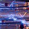
| Image shows lightning bolts travelling through the honeycomb motif, symbolizing the fast, confined flow of electrons in HfSn₂. A DNA-like helix represents the chiral stacking that locks these motifs together, protecting the two-dimensional character of the electronic flow despite the material’s three-dimensional bonding. (Image: Dr Jonathan Alaria).
|
|
The work was jointly led by Dr Jonathan Alaria (Physic), and Professor Matthew Rosseinsky OBE FRS, (Chemistry), highlighting the essential synergy between physics and chemistry that underpins this discovery. The team used a combination of theoretical modelling and experiments on high‑quality single crystals grown in the laboratory. Here researchers showed that HfSn₂ contains honeycomb layers arranged in three dimensions in a special chiral stacking pattern (similar to the twist in DNA). This arrangement preserves the unique electronic behaviour normally seen only in 2D materials.
|
|
These honeycomb layers also allow the material to host Weyl points – unusual points in the electronic structure that can dramatically enhance how easily electrons move. As a result, electrons in HfSn₂ act as if they are travelling in a 2D material, even though the structure itself is fully 3D.
|
|
The paper’s key finding is that the way electrons move in HfSn₂ can behave like a 2D system, even though the atoms form a strong 3D network. This means the electronic behaviour can be separated from the actual structure of the material. It also shows that 2D‑like performance is possible in materials that are much more robust than typical layered crystals.
|
|
The HfSn₂ study demonstrates how carefully controlling chemical bonding and stacking patterns in direct physical space can be used to tune electronic behaviour in energy–momentum space.
|
|
Dr Jonathan Alaria, Senior Lecturer in Physics at the University of Liverpool, said: “Our work shows that 2D‑like electronic transport can be realised within a fully 3D material. Demonstrating this required advanced physics experiments under extreme conditions, combined with close collaboration with our chemistry colleagues. This synergy was vital and we could only uncover these new concepts by uniting theoretical modelling, crystal growth and high‑field transport measurements.”
|
|
Professor Matt Rosseinsky concluded: “We asked ourselves, do materials need to be two‑dimensional to behave like graphene, or can we create graphene‑like properties in completely different kinds of materials with higher structural dimensions? These results show the power of chemistry to generate counter-intuitive properties by controlling the atomic arrangements that determine function and suggest there may be broader opportunities to generate two-dimensional high mobility for low-energy electronic devices beyond reliance on structurally layered materials.”
|