Identical growth conditions yield uniform monolayer graphene on three different perovskite oxides, suggesting gas-phase chemistry enables universal fabrication without the defects that transfer methods introduce.
(Nanowerk Spotlight) Stacking graphene onto perovskite oxides creates hybrid structures with electronic properties that neither material possesses alone. Graphene on strontium titanate, for example, exhibits a helical quantum Hall phase and magnetoresistance behaviors that have made it a standard platform for probing two-dimensional electron physics. But building these hybrids cleanly has been an obstacle that conventional methods cannot overcome.
The standard fabrication sequence requires growing graphene on copper foil, coating it with polymer for mechanical support, etching away the copper, pressing the graphene onto the target oxide, and dissolving the polymer. The process is tedious and unreliable. Polymer residues cling to surfaces. Mechanical handling tears the single-atom lattice. Wrinkles form where the sheet buckles. Even successful transfers produce interfaces compromised by contamination and structural damage.
Direct growth would bypass these problems, but insulating oxides offer none of the catalytic assistance that makes graphene synthesis on metals straightforward. Copper surfaces break down hydrocarbon gases and feed carbon atoms into a growing sheet. Oxides cannot do this.
Without surface catalysis, growth depends on thermal decomposition at extreme temperatures, and past attempts produced inconsistent results: patchy coverage on some substrates, multilayer clumps on others, with each material seemingly demanding its own optimization.
Researchers at Sungkyunkwan University in South Korea, working with collaborators at the University of Tennessee and other institutions, have now demonstrated that a single set of growth conditions works across multiple oxide substrates.
Their results, published in the journal Small Structures (“Universal Fabrication of Graphene/Perovskite Oxide Hybrid Heterostructures”), show uniform monolayer graphene on three chemically distinct perovskite oxides using identical parameters in atmospheric pressure chemical vapor deposition (APCVD). The substrates require no individual tuning. The same temperature, the same gas mixture, the same timing produces equivalent results on all three.
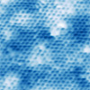
Uniform graphene growth on (a–c) STO and (d–f ) LAO substrates. (a,d) Representative Raman spectra from 16 evenly spaced points on the HH surfaces, demonstrating graphene uniformity. The positions of the measured points are marked as different colors and numbers on the optical microscopy images in (b,e) (scale bar: 1 mm). (c,f ) 2D intensity mappings of Raman spectra from the HHs taken at random positions (scale bar: 4 μm). (Image: Reproduced from DOI:10.1002/sstr.202500613, CC BY) (click on image to enlarge)
The team tested strontium titanate (SrTiO₃), lanthanum aluminate (LaAlO₃), and LSAT, a mixed perovskite containing lanthanum, strontium, aluminum, and tantalum. All three are widely used in oxide electronics research and remain stable above 1100 °C, a prerequisite for the high-temperature process. The researchers flowed argon, hydrogen, and methane through a quartz tube furnace at atmospheric pressure, positioning substrates at the center of the heating zone.
Temperature determined success or failure. At 1070 °C, with gas flows of 250, 10, and 8 sccm for argon, hydrogen, and methane respectively, graphene formed as a continuous monolayer across the full 5 × 5 mm² substrate area. At 1060 °C, no graphene appeared. Above 1070 °C, adlayer formation began, becoming increasingly prominent at higher temperatures and leading to multilayer growth.
The optimal window proved narrow but robust. Growth times between 1 and 3 hours gave equivalent results, and at the optimal temperature a self-limiting process appeared to halt growth after one layer completed on clean surfaces.
An additional experiment reinforced this picture. The researchers placed substrates at different positions along the furnace tube. Near the gas inlet, where temperatures were lower, no growth occurred. At the center, where temperature peaked, optimal monolayer graphene formed. Toward the outlet, where reactive species accumulated, overgrowth and multilayer formation dominated. This gradient demonstrated that both temperature and radical concentration govern growth quality.
The researchers attribute this behavior to gas-phase chemistry rather than surface reactions. At 1070 °C, hydrogen radicals collide with methane molecules and strip away hydrogen atoms, generating methyl radicals. These reactive species drift to the substrate and assemble into graphene. Because the critical chemistry occurs in the gas rather than on the oxide surface, the substrate’s composition matters less than its thermal stability. The activation energy for methyl radical formation, between 45 and 60 kJ/mol, lies well within reach at the growth temperature. This mechanism accounts for why one protocol succeeds on three different oxides.
Multiple techniques confirmed graphene quality. Raman spectroscopy detects characteristic vibrational signatures that serve as fingerprints for carbon materials. The D, G, and 2D peaks measured at 16 points across each substrate showed the consistent pattern expected from uniform monolayer graphene. X-ray absorption spectroscopy verified carbon-carbon bonding consistent with graphene rather than graphene oxide or disordered carbon.
Atomic force microscopy revealed nanoscale flatness, with surface roughness below 0.32 nm across all samples. Line features 0.6 to 1.2 nm tall correspond to wrinkles that form during cooling as graphene and substrate contract at different rates. Cross-sectional transmission electron microscopy confirmed these wrinkles do not break the graphene sheet; the monolayer remains continuous even where it buckles. The images showed graphene sitting approximately 0.4 nm above the oxide surface, with multilayer regions appearing only at pre-existing substrate defects.
Beyond confirming successful growth, the team found evidence that graphene and substrate interact electronically and mechanically. Raman spectra collected while cooling a graphene-on-strontium-titanate sample revealed an anomaly near 100 K, where strontium titanate undergoes a known structural distortion. The graphene’s vibrational frequencies shifted in response to strain transmitted from the transitioning substrate. Graphene on lanthanum aluminate showed no such feature, consistent with that oxide’s lack of a low-temperature phase transition.
Scanning tunneling microscopy at 4.2 K resolved individual carbon atoms in the honeycomb lattice and probed local electronic structure. Electrons had transferred from the oxide into the graphene, pushing its charge neutrality point below the measurement energy and indicating substantial doping.
A gap-like feature spanning approximately 130 mV at the Fermi level reflected phonon-mediated tunneling, where electrons excite lattice vibrations as they enter the surface. These coupled behaviors confirm that the graphene does not merely sit on the oxide but interacts with it, the condition required for the hybrid quantum phenomena that make these structures valuable.
The practical significance is a fabrication route that eliminates transfer entirely. Demonstrating that identical conditions produce equivalent graphene on three different perovskite oxides supports the proposed gas-phase mechanism and suggests that other thermally stable insulators may work without further optimization. For researchers building devices based on graphene-oxide hybrids, from quantum electronic systems to advanced sensors, this offers a path to cleaner interfaces and more reproducible results than transfer methods have provided.
For authors and communications departmentsclick to open
Lay summary
Prefilled posts
Nanowerk Newsletter
Get our Nanotechnology Spotlight updates to your inbox!
Thank you!
You have successfully joined our subscriber list.
Become a Spotlight guest author! Join our large and growing group of guest contributors. Have you just published a scientific paper or have other exciting developments to share with the nanotechnology community? Here is how to publish on nanowerk.com.