Redefining the repeating pattern in photonic crystals creates tightly confined pathways for light while preserving symmetry, offering a simple route to ultracompact and low loss light circuits.
(Nanowerk Spotlight) Topological photonics is built on the idea that light can be guided through materials in a way that resists defects and irregularities. The field borrows inspiration from electronic systems that exhibit the quantum Hall effect, where electrons flow along protected edges even in the presence of disorder. Unlike electrons, photons do not experience magnetic fields in ordinary materials, so researchers have looked for geometric ways to mimic that behavior.
The most common strategy has been to design photonic crystals, which are periodic patterns of holes or rods in a dielectric slab that support interface states along their boundaries. These states can carry light efficiently while remaining stable against small imperfections in the structure. Experiments have shown that such designs can route light around sharp corners, slow it down, and even form cavities for lasing. Yet practical integration on a chip has remained difficult.
Most topological photonic devices rely on breaking inversion symmetry, meaning the crystal is designed so that each hole is not a mirror image across the unit cell. This is usually achieved by altering hole sizes or positions. Doing so creates what physicists call Berry curvature, which describes how the wave patterns of light twist as they move through the crystal’s momentum space.
Berry curvature acts like an effective magnetic field for photons, steering them in a way that allows light to be guided along protected channels at the interface between two regions. This effect, known as topological transport, ensures that the light can keep moving even in the presence of small imperfections.
However, reshaping holes produces strong electric fields that extend beyond the guiding region. These stray fields limit confinement and cause leakage, making it difficult to pack many channels close together or to stack multiple layers in three-dimensional architectures.
Another issue is polarization. Many demonstrations emphasize transverse electric (TE) modes, where the electric field lies mostly in the plane of the crystal. These modes are easier to excite but harder to confine in metal–dielectric stacks, where energy tends to escape vertically. Transverse magnetic (TM) modes, with their dominant electric field pointing out of the plane, offer stronger isolation in metal-cladded structures, but designing topological states for them has proven more elusive.
Instead of physically breaking inversion symmetry, Yi Ji Tan and Ranjan Singh from the University of Notre Dame, redefine the unit cell—the repeating tile that describes the lattice. By shifting the unit cell boundary so that it possesses threefold rotational symmetry (C3) rather than the more typical sixfold symmetry (C6), they generate nonzero Berry curvature even though the bulk crystal remains inversion symmetric.
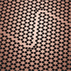
Emergent Berry curvature in photonic crystal with bulk inversion symmetry enables TM-polarized topological interface state on a chip. a) Defining a photonic crystal unit cell with 6-fold rotational symmetry results in zero Berry curvature for the lower TM-polarized photonic band. b) Unit cell boundary is redefined to create Type I and II unit cell with 3-fold rotational symmetry, where nonzero Berry curvature localization emerges at the high-symmetry K and K’ points with opposite polarity (red – positive, blue – negative). c) Alternative diamond-shaped Type I and II unit cell for forming glide-symmetric interfaces. d) The unit cell in (a) is unable to form interfaces. Any local defects can be deformed to restore the global periodicity. e) Hexagon unit cells in (b) form a glide-symmetric interface. Global periodicity cannot be restored via local deformations. However, the presence of pentagon air holes is not suitable for the efficient coupling of THz waves using a taper. f) Diamond unit cells in (c) form a similar glide-symmetric bearded interface without air holes. g) A bearded interface waveguide with sharp bends in a photonic crystal chip with bulk inversion symmetry. The photonic crystal is a 200 μm thick silicon enclosed between 500 nm copper films with a unit cell of 165 μm period and two hexagon air holes of 47.6 μm radius. h) TM-polarized projected band diagram of the bearded interface in (f), computed using the refractive index of 3.45 for a 200 μm thick slab enclosed between perfect electric conductors. i) Measured transmittance of the photonic crystal waveguide chip with and without bends. (Image: Reprinted from DOI:10.1002/adma.202508651, CC BY(click on image to enlarge)
Berry curvature is a mathematical quantity that describes how the phase of a wave twists when its momentum changes. In electronic systems, it acts like a magnetic field in momentum space, leading to the Hall effect. In photonics, it can give rise to valley-dependent behavior, where two points in the crystal’s momentum space, labeled K and K′, carry opposite curvature. A domain wall between regions of opposite curvature can host a guided state that resists scattering. The innovation here is showing that such curvature can appear purely from how the unit cell is defined, rather than from altering the holes.
The paper demonstrates this idea using a honeycomb lattice of hexagonal holes. If the unit cell is defined with C6 symmetry, the TM band structure shows no Berry curvature. Redefining it with C3 symmetry, however, produces sharply localized curvature at the K and K′ valleys. The researchers calculate valley Chern numbers of about ±0.033, small but finite, signaling that topological interface states should appear. Unlike earlier valley photonic crystals, which required physical asymmetry, this method leaves the hole geometry untouched.
Building on this foundation, the team designs interfaces that exploit the curvature difference between domains. They first explore a glide symmetric interface, where the pattern repeats after a reflection and a half-period translation. While effective, this design leaves pentagon-shaped holes at the boundary, complicating coupling from a standard waveguide.
To address that, they propose a “bearded” interface defined by diamond-shaped unit cells with shifted holes, creating a continuous channel without boundary holes. Both versions support a single TM-guided mode confined to the interface.
Numerical simulations show that the bearded interface supports a linear dispersion band within the gap, with a bandwidth of about 49 gigahertz. The guided field remains tightly confined within one unit cell across the channel, about one-fifth of the operating wavelength. This is much stronger confinement than in conventional valley photonic crystals and is crucial for routing light along compact paths with minimal leakage.
To test the concept experimentally, the researchers fabricated a waveguide using silicon sandwiched between copper films, creating a metal–dielectric–metal structure. The silicon slab is 200 micrometers thick, with a lattice period of 165 micrometers and hexagonal holes of radius 47.6 micrometers. The copper layers, only 500 nanometers thick, act as near-perfect conductors at terahertz frequencies and prevent energy from escaping vertically. Light is coupled into the device through a tapered silicon input attached to a hollow metallic waveguide.
Measurements show strong transmission over a band from 300 to 400 gigahertz, matching simulations. The interface channel guides light through sharp S-bends with radii less than one-quarter of the wavelength, a scale difficult to achieve in earlier designs. Losses remain low even in these tight bends. Only three rows of photonic crystal holes on each side of the interface are needed to isolate the guided mode, a direct result of the ultracompact confinement enabled by the C3 unit cell design.
The team quantified losses in both straight and bent sections. Simulations indicate about 0.14 decibels per millimeter at 395 gigahertz in straight sections, dominated by resistive heating in the copper. For S-bends of the same length, the loss rises slightly to 0.19 decibels per millimeter, less than 0.05 decibels per bend. Measured samples show higher values—about 0.40 decibels per millimeter in straight segments—due to fabrication misalignments. Even so, bend-induced loss is negligible, which is critical for dense routing on a chip.
Beyond the honeycomb lattice, the researchers explore the generality of the approach. They show that redefining the unit cell from C6 to C3 symmetry induces Berry curvature in multiple lattice types, not just honeycomb. In triangular lattices, for example, TE polarization can produce curvature when the unit cell is chosen with C3 symmetry. With triangular holes, the geometry itself breaks inversion symmetry and creates curvature directly, while with hexagonal holes the outcome depends entirely on unit cell definition.
This demonstrates that the method is not tied to a specific geometry or polarization but represents a broader principle: the way one defines the repeating tile of the crystal can create effective asymmetry, even if the bulk remains symmetric.
This principle has important implications for photonic integration. In-plane isolation arises because the topological interface state is confined within a large bandgap of the surrounding crystal, ensuring that light does not leak laterally. Out-of-plane isolation comes from the metal cladding, which prevents radiation loss into free space. Together, these features create ultraconfined channels that remain both laterally and vertically contained.
The work also clarifies how topological features depend on polarization and lattice structure. For TE modes in honeycomb lattices, Dirac cones appear when inversion and time-reversal symmetry are preserved, and breaking inversion symmetry by hole deformation opens a gap and produces Berry curvature.
For TM modes, the situation differs: Dirac cones appear in triangular lattices, but Berry curvature in honeycomb lattices emerges only when the unit cell is redefined. Recognizing this distinction helps explain why the new C3 unit cell approach leads to strong confinement and robust waveguiding for TM polarization.
From an engineering perspective, the contribution is twofold. It introduces a symmetry-based recipe for generating Berry curvature without altering the bulk, simplifying fabrication and aligning with silicon photonics processes. It also demonstrates a working device that routes terahertz light through ultracompact, low-loss channels capable of sharp bends and dense integration.
By showing that Berry curvature can emerge purely from unit cell definition, the study expands the design space of topological photonics. It points to practical routes for building chip-scale systems where light can be directed with high precision and low loss, even in geometrically constrained layouts. Because the method does not depend on tailoring hole sizes or shapes, it can be readily adapted to different materials and lattice types. This conceptual shift—from reshaping the bulk to redefining the unit cell—may provide the flexibility needed to integrate topological photonics into compact, manufacturable platforms for terahertz technologies and beyond.
For authors and communications departmentsclick to open
Lay summary
Prefilled posts
Nanowerk Newsletter
Get our Nanotechnology Spotlight updates to your inbox!
Thank you!
You have successfully joined our subscriber list.
Become a Spotlight guest author! Join our large and growing group of guest contributors. Have you just published a scientific paper or have other exciting developments to share with the nanotechnology community? Here is how to publish on nanowerk.com.