Ultrafast laser processing creates silicon surfaces that absorb nearly all infrared light and remain stable under heat and wear, enabling coating-free infrared sensing and calibration.
(Nanowerk Spotlight) Blackbodies are used as physical reference sources in technologies that detect heat and infrared light. A blackbody is not a specific material but an ideal surface defined in physics as one that absorbs all incoming radiation and emits energy based only on its temperature. Although no real object behaves this way perfectly, blackbody models are essential for understanding how heat is radiated and for interpreting thermal signals.
In practice, blackbody-like surfaces are built to calibrate instruments such as infrared cameras, thermal sensors, and remote-sensing satellites. These surfaces act as controlled standards, allowing devices to convert incoming radiation into accurate temperature readings. The closer a material comes to blackbody behavior, the more precisely it can be used to measure or simulate thermal emission in systems where direct contact is not possible.
But building a surface that consistently absorbs radiation across a wide range of infrared wavelengths is far from simple. Most designs rely on coatings or layered materials that perform well in the lab but degrade under heat, abrasion, or long-term exposure. Others use microstructured surfaces that are efficient but fragile or limited in spectral range. The result is a persistent tradeoff between optical performance and environmental durability, especially in systems that operate under harsh conditions.
In a single processing step, the laser treatment forms a dense array of microscopic cones and creates atomic-scale defects just beneath the surface. Together, these features allow the treated surface to absorb over 98 percent of infrared radiation across the 3 to 14 micrometer range. The surface remains stable after exposure to temperatures above 900 degrees Celsius and withstands repeated mechanical wear, offering a potential solution to the limitations of conventional blackbody sources.
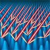
Principle of back-scattering suppression. a) Schematic of the fs-laser-induced hierarchical silicon micro-cone array covered by nanoparticles (NPs). b) Simulated back-scattering cross-section patterns of small (0.2 μm), medium (0.5 μm), and large size (1.2 μm) NPs. The colorful regions above the NPs depict the polarization-dependent differential scattering cross-sections, where the left and right half sides of the dashed lines represent the differential scattering cross-sections in the planes parallel with and perpendicular to the incident polarization, respectively. c) Simulated integral back-scattering cross-sections of a N-type silicon NP with respect to the particle size. The solid and dashed lines indicate the scattering cross-sections corresponding to 5% and 1%, respectively. d) The same as c, but for a silica NP. e) Schematic of the back-scattering angle suppression in the micro-cone array, where taller and steeper cones yield lower back-scattering angles. The inset shows the simulated reflectance spectra of a single N-type silicon NP (dashed lines) or silica NP (solid lines) with different back-scattering solid angles. f) Far-field reflectance spectra of a micro-cone array, as depicted in c, with period 30 μm and varied cone depth, which is covered by dense N-type silicon NPs. (Image: Reprinted with permission by Wiley-VCH Verlag) (click on image to enlarge)
The research addresses two core challenges that have historically limited blackbody performance. The first is how to reduce reflectivity across a broad spectral range. The second is how to ensure strong and uniform absorption without relying on added materials that may degrade over time. The method presented here uses a laser-based process to solve both problems simultaneously.
The laser pulses, each lasting just a few hundred femtoseconds, are used to write a repeating pattern of cone-shaped structures into the silicon surface. These cones are about 90 micrometers deep and spaced at regular 30 micrometer intervals. The geometry of the cones reduces back-scattering of incoming light, directing more of it into the material instead of allowing it to reflect away.
At the same time, the process generates nanoparticles roughly 200 nanometers in diameter that scatter light at angles favorable to absorption. The combined structure functions as a highly effective light trap without relying on any external layer or added film.
While the surface structure enhances optical trapping, the second effect of the laser processing improves the material’s intrinsic ability to absorb infrared light. The rapid heating and cooling caused by the pulses introduces a dense layer of nanometer-scale defects in the crystal lattice. These defects act as additional energy states within the silicon bandgap. Incoming infrared photons can excite electrons from these defect states into the conduction band, effectively increasing the range of photon energies the material can absorb. This process is known as defect-induced energy level engineering.
Spectroscopic measurements confirm that these defect states are responsible for a significant portion of the observed infrared absorption. Deep-level transient spectroscopy detected twelve distinct defect states created by the laser process. Transmission electron microscopy showed that the laser-affected region contains an amorphous silicon layer near the surface, followed by a polycrystalline region with high defect density, and finally transitions into the unaltered single crystal structure deeper in the wafer.
Importantly, the defects were introduced without oxygen contamination, which would otherwise affect stability. This was confirmed using elemental analysis after surface cleaning.
To quantify the contribution of each feature to the overall absorption, the researchers performed controlled comparisons using different sample treatments. Surfaces with both nanoparticles and laser-induced defects showed the highest absorption. Samples where the defects were removed by chemical etching, or where only nanoparticles were present without defect formation, exhibited significantly lower performance. This indicates that both structural and electronic modifications are essential for the high emissivity achieved.
In practical terms, the method offers several advantages over existing approaches. Because it does not involve coatings or additional materials, the surface is inherently more stable under mechanical and thermal stress. Durability tests showed no significant loss of emissivity after heating to 900 degrees Celsius or after repeated application and removal of adhesive tape.
Accelerated aging experiments suggest that the surfaces can maintain their performance for at least a decade under ambient conditions. Uniformity measurements across a 60 millimeter square sample showed emissivity variation of less than 0.25 percent, and the variation between different samples remained within 0.15 percent.
The laser processing itself is scalable and does not require vacuum conditions or cleanroom facilities. The researchers used a standard femtosecond laser system and controlled the energy density by defocusing the beam and using precise motion stages to scan the surface. A feedback effect during the process ensures that once the target geometry is reached, further laser passes do not significantly alter the structure. This self-limiting behavior helps achieve uniform results over large areas.
The surface design also shows minimal sensitivity to the angle of incoming light. Simulations and measurements demonstrated consistent performance across a wide range of incident angles, which is important for real-world applications where radiation may not always strike at normal incidence.
The paper’s contribution lies not in discovering a new material, but in demonstrating a new way of turning an existing one into a better approximation of an ideal blackbody. By integrating surface geometry and sub-surface defect engineering into a single manufacturing step, the method bypasses many of the common points of failure in conventional blackbody construction. This opens up possibilities for more robust and portable calibration targets, particularly in settings where coatings are unsuitable or maintenance is difficult.
The resulting surfaces are not perfect blackbodies, but they perform close enough to the ideal across a key spectral range to meet the demands of precision infrared systems. More importantly, they offer the combination of optical efficiency, structural integrity, and manufacturing scalability that current designs struggle to provide. For fields where infrared accuracy matters, this represents a practical advance that could improve the stability and reliability of core measurement tools.
For authors and communications departmentsclick to open
Lay summary
Prefilled posts
Nanowerk Newsletter
Get our Nanotechnology Spotlight updates to your inbox!
Thank you!
You have successfully joined our subscriber list.
Become a Spotlight guest author! Join our large and growing group of guest contributors. Have you just published a scientific paper or have other exciting developments to share with the nanotechnology community? Here is how to publish on nanowerk.com.