Uniform gaps below ten nanometers boost tuning range and efficiency in graphene metasurfaces for mid-infrared sensing, imaging, and communications.
(Nanowerk Spotlight) Picture a wafer-thin optical chip that can change its infrared color at will. Such a device could detect gases by their unique light signatures, steer beams for thermal imaging, or hide data within patterns invisible to the human eye.
The most promising platforms for this type of control are metasurfaces. These are flat layers patterned with arrays of tiny metal antennas that can bend, filter, or focus light. To make them tunable, researchers often combine them with graphene, a one-atom-thick layer of carbon whose conductivity can be changed by applying a voltage. This electrical control allows the optical response to be shifted in real time.
In principle, the tuning becomes much stronger when the antennas are placed extremely close together. The narrow space between them, called the gap, forces light into a concentrated region where it interacts more strongly with the graphene.
The problem is that standard top-down fabrication methods struggle to make gaps smaller than about twenty nanometers with high precision. Bottom-up chemical assembly can form narrower gaps, but these approaches are difficult to integrate with transistor-style devices and large-area patterns. This limitation has kept tunable metasurfaces from reaching their full potential.
Researchers from KU Leuven, imec, and collaborators have now developed a process that reliably creates uniform gaps below ten nanometers over practical device areas. They use it to build a graphene-metal hybrid metasurface that can shift its infrared resonance far more than devices made with wider gaps (Advanced Science, “Enhanced Spectral Tunability by Sub‐10 nm Nanogaps in Graphene‐Metal Hybrid Metasurfaces”).
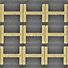
a) Schematic of the fabrication process illustrating the preparation of arrays of antennas that are separated by nanogaps. b) Measured nanogap size as a function of the nominal gap size for different thicknesses of the PVD Au layer. SEM images of c) LOM and d) IMM metasurfaces for different nominal gap sizes (scale bar, 200 nm). For the IMM metasurfaces a PVD Au thickness of 15 nm was used. e) Demonstration of the realisation of sub-10 nm gaps in different morphologies: rectangular-shaped (top), ‘I’-shaped (middle), and triangular-shaped (bottom) gold antenna arrays. The insets contain zoomed-in images around a single nanogap. (Image: Reprinted from DOI:10.1002/advs.202506898, CC BY) (click on image to enlarge)
The work matters because it tackles a key bottleneck in mid-infrared photonics. Devices operating in this part of the spectrum are important for environmental sensing, medical diagnostics, and free-space communications. Greater tunability means a single device can cover a wider range of wavelengths, reducing the need for multiple components.
The fabrication strategy starts with electron beam lithography to define pairs of gold antennas. These are patterned using lift-off processing, which produces an initial gap between each antenna pair. A thin aluminum oxide film is deposited before patterning to protect the graphene layer underneath.
Next, a thin extra layer of gold is added by physical vapor deposition. This coats the sidewalls of the antennas as well as their top surfaces. The final step is ion milling to remove the extra metal at the bottom of the gaps. The aluminum oxide layer acts as an etch stop so the graphene is not damaged. By adjusting the thickness of the added gold layer, the researchers can shrink the gaps from their original size to below ten nanometers.
This method produces consistent results over a sixty-micrometer square area and works with various antenna shapes. It is also compatible with the layered device structure needed for a graphene field-effect transistor.
A graphene field-effect transistor, or GFET, uses graphene as the conducting channel between two contacts. Applying a voltage to a gate electrode changes the number of charge carriers in the graphene. This alters how the graphene absorbs and reflects light, especially in the infrared.
In the devices built for this study, the graphene and antennas sit above a layer that forms a Fabry–Perot cavity. This optical cavity enhances absorption near a wavelength of eight micrometers. Electrical tests confirm that the GFETs behave normally, with a charge-neutrality point near sixty volts. After ion milling, the maximum sheet resistivity decreases slightly, which the authors attribute to small defects in the protective oxide.
Optical measurements reveal the benefit of the narrower gaps. Using a Fourier transform infrared microscope, the researchers measure how the resonance wavelength changes as they vary the gate voltage. In the widest-gap devices, the resonance shifts by about a quarter of a micrometer. In devices with thirty-nanometer gaps, the shift doubles to roughly half a micrometer.
With the new process, they create devices with eight-nanometer gaps. These show a shift of about 0.77 micrometers, the largest of the series. The improvement is consistent with simulations that show stronger electric fields in the narrow gaps. In the smallest-gap devices, the electric field in the graphene plane is about forty thousand times stronger than the incoming light field.
An equivalent circuit model supports the same conclusion. In this picture, reducing the gap lowers the effective inductance linked to the graphene, which increases the range over which the resonance can be tuned.
The devices also show higher modulation depth, which is the change in reflected light between the high and low voltage states. At a thirty-nanometer gap, the maximum modulation depth is about forty-five percent. At eight nanometers, it rises to nearly fifty-nine percent. These values outperform most reported mid-infrared modulators that work in free space.
The authors note that further gains could come from design refinements. Reducing ion beam energy, improving the quality of the oxide barrier, and smoothing metal edges could protect the graphene and limit optical losses. They also suggest adding a transparent top gate with a thin, high-permittivity dielectric to lower the operating voltage and increase the charge density in the graphene.
The broader message is straightforward. Narrowing the antenna gaps in a graphene–metal metasurface to below ten nanometers increases both the tuning range and the modulation efficiency. The process demonstrated here uses accessible fabrication steps and works over useful device areas.
The measured tuning range grows from 0.50 micrometers for wider gaps to 0.77 micrometers for the smallest. The modulation depth improves from forty-five to fifty-nine percent. These gains could make electrically tunable mid-infrared metasurfaces more practical for sensing, imaging, and communications systems that benefit from fast, adjustable control of light.
For authors and communications departmentsclick to open
Lay summary
Prefilled posts
Nanowerk Newsletter
Get our Nanotechnology Spotlight updates to your inbox!
Thank you!
You have successfully joined our subscriber list.
Become a Spotlight guest author! Join our large and growing group of guest contributors. Have you just published a scientific paper or have other exciting developments to share with the nanotechnology community? Here is how to publish on nanowerk.com.