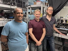
Home > Press > ICFO researchers overcome long-standing bottleneck in single photon detection with twisted 2D materials From left to right, Roshan Krishna Kumar, Frank Koppens and Krystian Nowakowski in their lab at ICFO. Credit Image Credit: ICFO Abstract:The ability to detect single photons (the smallest energy packets constituting...
Nanotechnology Now – Press Release: Simple algorithm paired with standard imaging tool could predict failure in lithium metal batteries

Home > Press > Simple algorithm paired with standard imaging tool could predict failure in lithium metal batteriesAbstract:Researchers at the University of California San Diego have developed a simple yet powerful method to characterize lithium metal battery performance with the help of a widely used imaging tool: scanning electron microscopy....
AI designs light-shaping surfaces in seconds for vivid holograms and adaptable optics

Aug 09, 2025 AI model designs complex metasurfaces in seconds using physics-guided learning, enabling rapid, high-quality holographic devices and adaptable optical systems for multiple wavelengths and polarizations. (Nanowerk Spotlight) Imagine a holographic display as thin as a sheet of glass, projecting crisp, full-color 3D images without lenses or bulky optics....
Nanotechnology Now – Press Release: New molecular technology targets tumors and simultaneously silences two undruggable cancer genes

Home > Press > New molecular technology targets tumors and simultaneously silences two undruggable cancer genes Targeting two cancer-causing genes at the same time is akin to slicing both Achilles heels of cancer, which has tremendous potential, said Chad V. Pecot, MD, corresponding author of the article, professor of medicine...
Nanotechnology Now – Press Release: Lab to industry: InSe wafer-scale breakthrough for future electronics
Home > Press > Lab to industry: InSe wafer-scale breakthrough for future electronicsAbstract:In a landmark advancement for next-generation electronics, researchers from the International Center for Quantum Materials at Peking University in collaboration with Renmin University of China have successfully fabricated wafer-scale two-dimensional indium selenide (InSe) semiconductors. Led by Professor Liu...
Nanotechnology Now – Press Release: First real-time observation of two-dimensional melting process: Researchers at Mainz University unveil new insights into magnetic vortex structures
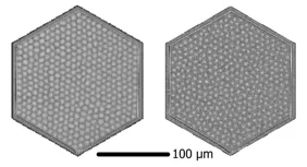
Home > Press > First real-time observation of two-dimensional melting process: Researchers at Mainz University unveil new insights into magnetic vortex structures Snapshots of the skyrmion lattice during the melting: an ordered skyrmion lattice on the left while the lattice structure has vanished on the right. Credit photo/: Raphael...
Nanotechnology Now – Press Release: New imaging approach transforms study of bacterial biofilms

Home > Press > New imaging approach transforms study of bacterial biofilms This artistic rendering depicts an atomic force microscopy tip scanning a structured network of bacterial cells with flagella in a honeycomb pattern. High-resolution surface characterization spans a wide field of view. Credit Adam Malin/ORNL, U.S. Dept....