
Sep 05, 2022 (Nanowerk Spotlight) The silicon-based CMOS technology is fast approaching its physical limits, and the electronics industry is urgently calling for new techniques to keep the long-term development. Two-dimensional (2D) semiconductors, like transition-metal dichalcogenides (TMDs), have become a competitive alternative to traditional semiconducting materials in the post-Moore era,...
Uncovering the atomic mechanism underpinning heat transport in thermoelectric materials
Sep 03, 2022 (Nanowerk News) Thermoelectric devices convert thermal energy into electricity by generating a voltage from the difference in temperature between the hot and cold parts of a device. To better understand how the conversion process occurs at the atomic scale, researchers used neutrons to study single crystals of...
Motion of DNA linked to its damage response, ability to repair itself

Sep 03, 2022 (Nanowerk News) A multidisciplinary team of Indiana University researchers have discovered that the motion of chromatin, the material that DNA is made of, can help facilitate effective repair of DNA damage in the human nucleus -- a finding that could lead to improved cancer diagnosis and treatment....
Multilayer stack opens door to low-power electronics
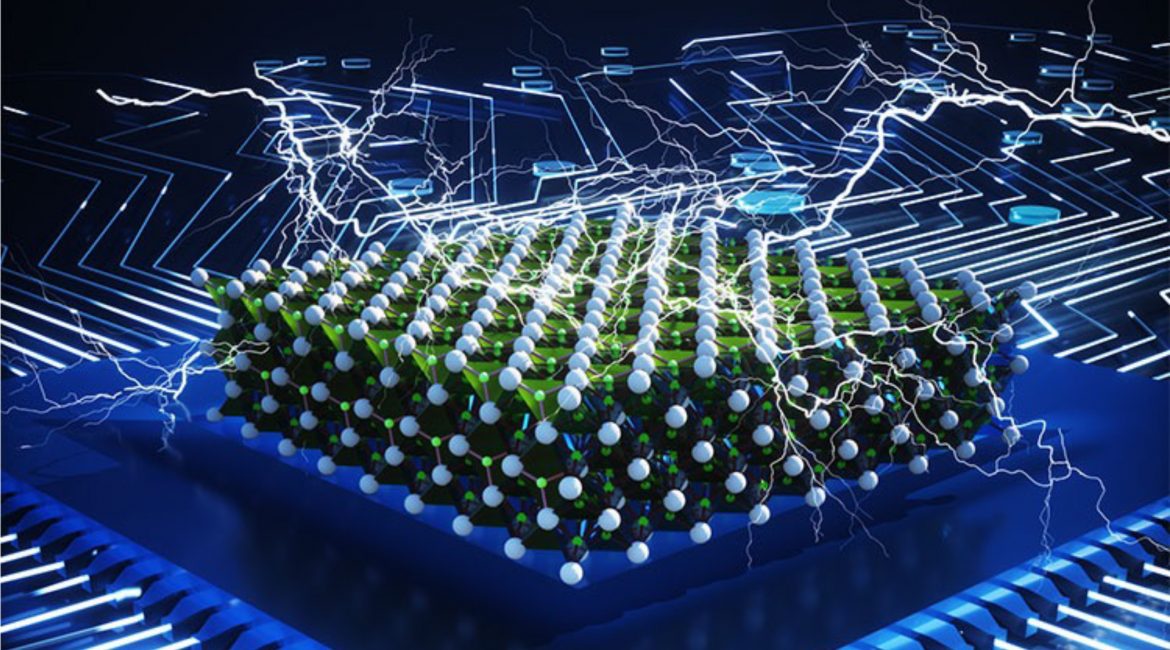
Sep 03, 2022 (Nanowerk News) Researchers found that a stack of ultrathin materials, characterized in part at the Advanced Light Source (ALS), exhibits a phenomenon called negative capacitance, which reduces the voltage required for transistor operation (Nature, "Ultrathin ferroic HfO2-ZrO2 superlattice gate stack for advanced transistors"). The material is fully...
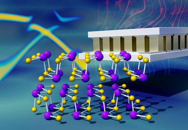
Van der Waals infrared photodetectors based on ‘optical’ and ‘electrical’ combined manipulations
Sep 02, 2022 (Nanowerk Spotlight) Blackbody response is highly desired in two-dimensional (2D) infrared photodetectors, which determines their practical applications. State-of-the-art available blackbody response mid-wavelength infrared (MWIR) photodetectors are fabricated using materials such as HgCdTe, InSb and InAsSb. However, these photodetectors need to operate at cryogenic temperatures to minimize thermally...
Team measures electronic noise more precisely than ever before
Sep 02, 2022 (Nanowerk News) A team of DESY scientists has succeeded for the first time in measuring so-called phase noise with 500 times greater precision than has been technically achievable in this frequency range before (IEEE Transactions on Instrumentation and Measurement, "Phase Noise Measurements for L-Band Applications at Attosecond...
Physicists develop a linear response theory for open systems having exceptional points

Sep 02, 2022 (Nanowerk News) Linear analysis plays a central role in science and engineering. Even when dealing with nonlinear systems, understanding the linear response is often crucial for gaining insight into the underlying complex dynamics. In recent years, there has been a great interest in studying open systems that...
New study confirms ‘rippled sheet’ protein structure predicted in 1953

Sep 02, 2022 (Nanowerk News) An unusual protein structure known as a “rippled beta sheet,” first predicted in 1953, has now been created in the laboratory and characterized in detail using x-ray crystallography. The new findings, published in Chemical Science ("The rippled b-sheet layer configuration – a novel supramolecular architecture...
entanglement of many atoms discovered for the first time

Sep 02, 2022 (Nanowerk News) Be it magnets or superconductors: materials are known for their various properties. However, these properties may change spontaneously under extreme conditions. Researchers at the Technische Universität Dresden (TUD) and the Technische Universität München (TUM) have discovered an entirely new type of such phase transitions. They...
Webb telescope takes its first-ever direct image of distant world

Sep 02, 2022 (Nanowerk News) For the first time, astronomers have used NASA’s James Webb Space Telescope to take a direct image of a planet outside our solar system. The exoplanet is a gas giant, meaning it has no rocky surface and could not be habitable. The image, as seen...