| Jun 09, 2026 |
Researchers designed a twisted 2D conductive MOF that preserves its electronic properties when stacked, advancing practical 2D materials.
(Nanowerk News) Two-dimensional (2D) materials, which are significantly thinner than a single sheet of paper, have long drawn attention for their exceptional performance. However, they have faced a critical limitation: their performance degrades significantly when multiple layers are stacked.
|
|
A research team at KAIST has successfully resolved this long-standing bottleneck by developing a new conductive material that retains its single-layer electronic characteristics even when stacked in multiple layers. This breakthrough is expected to accelerate the commercialization of next-generation electronic devices and quantum materials.
|
|
The research team led by Professor Sarah S. Park from the Department of Chemistry, in collaboration with Professor Christopher H. Hendon from the University of Oregon, has developed a new 2D conductive Metal-Organic Framework (MOF). This novel material maintains high electrical conductivity while minimizing interlayer interference (Journal of the American Chemical Society, “Homoconjugation-Enabled Kagome Bands in a Layer-Decoupled Two-Dimensional Conductive Triptycene-Based Metal–Organic Framework”).
|
|
Because 2D materials are atomically thin, electrons can move through them at ultra-high speeds, making them prime candidates for next-generation semiconductors and quantum materials. However, for practical applications, multiple layers must be stacked. When this happens, interlayer interactions obstruct electron movement, leading to performance degradation—similar to how cars driving fast on separate roads experience traffic congestion at an intersection.
|
|
In particular, while 2D conductive MOFs exhibit outstanding performance in their single-layer state, their inherent electronic properties weaken in the bulk state, where multiple layers are piled up.
|
|
To solve this problem, the research team focused on the “angle” of alignment to prevent the layers from directly interfering with each other. The newly designed molecular structure ensures that even when multiple layers are stacked, each layer is arranged at a specific angle, minimizing direct face-to-face contact. This operates on a similar principle to stacking a deck of cards with a slight twist rather than flushing them perfectly, preventing them from sticking together.
|
|
As a result, interlayer interactions were reduced, allowing electrons to move more freely. To achieve this structure, the team designed a triptycene-based molecule and used it to synthesize the new 2D conductive MOF material.
|
|
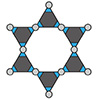
The newly developed material, named Ni₃(HITrip)₂ was found to preserve an electronic structure highly similar to that of a single layer, even in a multi-layered state. Notably, it retained a unique electronic structure (the Dirac band structure of a Kagome lattice) that allows electrons to move rapidly and efficiently. This structure is highly advantageous for achieving high electrical conductivity, enabling electrons to travel at high speeds as if on a highway without complex obstacles. This demonstrates that an electronic structure previously thought to be achievable only in a single layer can now be maintained in actual multi-layered bulk materials.
|
 |
| Schematic comparison of conventional planar-linker and triptycene-based 2D conductive MOFs, showing how twisted linkers suppress π–π interactions and enable 2D charge transport in stacked layers. (Image: KAIST) (click on image to enlarge)
|
|
In fact, this material exhibited a high electrical conductivity of 0.58 S/cm without any additional doping (a process of introducing impurities to enhance electrical properties), proving that excellent electrical performance can be achieved while mitigating interlayer interference.
|
|
Through computational modeling and spectroscopic analysis, the research team also uncovered the underlying mechanism behind this high conductivity. They confirmed that within the material, the molecules and metal atoms work cooperatively to facilitate electron transport, creating a stable environment for electron movement.
|
|
This study holds great significance as it resolves a long-standing challenge in 2D materials: the phenomenon where “stacking degrades performance.” By demonstrating that superior electronic properties previously limited to single layers can be realized in bulk materials, this research marks a vital turning point in connecting fundamental research to practical technology.
|
|
The research team anticipates that these findings will be widely utilized in the development of high-performance electronic devices and next-generation energy materials. Furthermore, by opening new possibilities for research into quantum materials and topological materials (next-generation functional materials with unique electron transport properties), this breakthrough is expected to contribute significantly to the advancement of future semiconductor and quantum information technologies.
|
|
Crucially, because the material retains its excellent electronic properties even when stacked, it will broaden the scope of functional material design required for manufacturing actual devices.
|
|
Professor Sarah S. Park stated, “This research demonstrates that 2D electronic structures, which were previously thought to be possible only in single layers, can now be realized in bulk materials. By precisely controlling interlayer interactions, a new pathway will open for implementing diverse quantum properties and electronic characteristics in practical materials.”
|